ISL84541IUZ データシートの表示(PDF) - Intersil
部品番号
コンポーネント説明
メーカー
ISL84541IUZ Datasheet PDF : 16 Pages
| |||
ISL84541, ISL84542, ISL84543, ISL84544
Absolute Maximum Ratings
V+ to GND . . . . . . . . . . . . . . . . . . . . . . . . . . . . . . . . . . . . -0.3 to15V
Input Voltages
IN (Note 3). . . . . . . . . . . . . . . . . . . . . . . . . . . -0.3 to ((V+) + 0.3V)
NO, NC (Note 3) . . . . . . . . . . . . . . . . . . . . . . -0.3 to ((V+) + 0.3V)
Output Voltages
COM (Note 3) . . . . . . . . . . . . . . . . . . . . . . . . -0.3 to ((V+) + 0.3V)
Continuous Current (Any Terminal) . . . . . . . . . . . . . . . . . . . . . 10mA
Peak Current, IN, NO, NC, or COM
(Pulsed 1ms, 10% Duty Cycle, Max) . . . . . . . . . . . . . . . . . . 20mA
ESD Rating (Per MIL-STD-883 Method 3015). . . . . . . . . . . . . .>2kV
Operating Conditions
Temperature Range
ISL8454XCX . . . . . . . . . . . . . . . . . . . . . . . . . . . . . . . . 0oC to 70oC
ISL8454XIX . . . . . . . . . . . . . . . . . . . . . . . . . . . . . . . . -40oC to 85oC
Thermal Information
Thermal Resistance (Typical, Note 4)
θJA (oC/W)
6 Ld SOT-23 Package . . . . . . . . . . . . . . . . . . . . . . .
230
8 Ld SOT-23 Package . . . . . . . . . . . . . . . . . . . . . . .
215
8 Ld MSOP Package . . . . . . . . . . . . . . . . . . . . . . . .
210
8 LD SOIC Package . . . . . . . . . . . . . . . . . . . . . . . . .
170
8 LD PDIP Package . . . . . . . . . . . . . . . . . . . . . . . . .
140
Maximum Junction Temperature (Plastic Package) . . . . . . . . 150oC
Moisture Sensitivity (See Technical Brief TB363)
All Other Packages. . . . . . . . . . . . . . . . . . . . . . . . . . . . . . . Level 1
8 Ld SOT-23 Package . . . . . . . . . . . . . . . . . . . . . . . . . . . . Level 2
Maximum Storage Temperature Range . . . . . . . . . . . . -65oC to 150oC
Maximum Lead Temperature (Soldering 10s) . . . . . . . . . . . . 300oC
(SOIC, MSOP and SOT-23 - Lead Tips Only)
CAUTION: Stresses above those listed in “Absolute Maximum Ratings” may cause permanent damage to the device. This is a stress only rating and operation of the
device at these or any other conditions above those indicated in the operational sections of this specification is not implied.
NOTES:
3. Signals on NC, NO, COM, or IN exceeding V+ or GND are clamped by internal diodes. Limit forward diode current to maximum current ratings.
4. θJA is measured with the component mounted on a low effective thermal conductivity test board in free air. See Tech Brief TB379 for details.
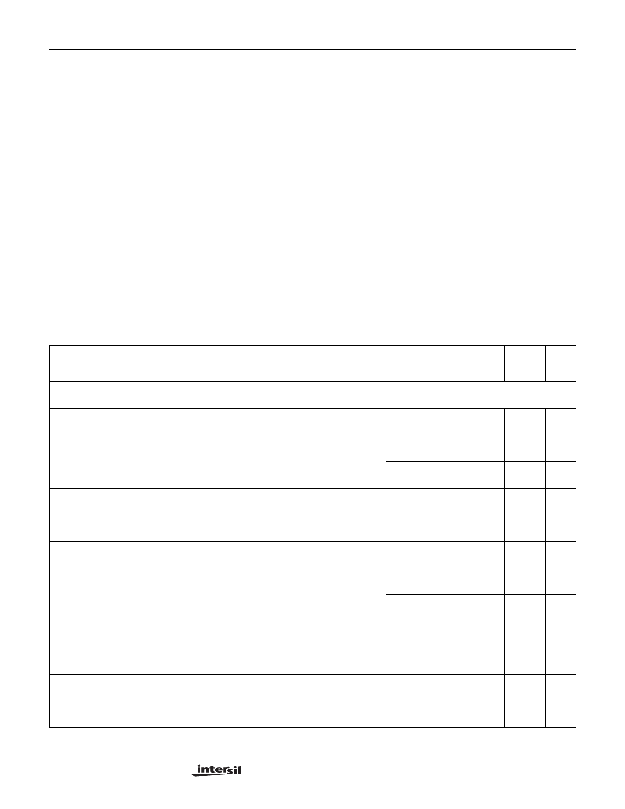
Electrical Specifications - 5V Supply Test Conditions: V+ = +4.5V to +5.5V, GND = 0V, VINH = 2.4V, VINL = 0.8V (Note 5),
Unless Otherwise Specified
PARAMETER
TEST CONDITIONS
TEMP MIN
MAX
(oC) (NOTE 6) TYP (NOTE 6) UNITS
ANALOG SWITCH CHARACTERISTICS
Analog Signal Range, VANALOG
ON Resistance, RON
V+ = 4.5V, ICOM = 1.0mA, VNO or VNC = 3.5V,
See Figure 5
Full
0
25
-
Full
-
-
V+
V
30
60
Ω
-
75
Ω
RON Matching Between Channels, V+ = 5V, ICOM = 1.0mA, VNO or VNC= 3.5V
∆RON
25
-
0.8
2
Ω
Full
-
-
4
Ω
RON Flatness, RFLAT(ON)
V+ = 5V, ICOM = 1.0mA, VNO or VNC = 1V, 2V, 3V
Full
-
NO or NC OFF Leakage Current, V+ = 5.5V, VCOM = 1V, 4.5V, VNO or VNC = 4.5V, 1V, 25
-0.1
INO(OFF) or INC(OFF)
Note 7
Full
-5
7
0.01
-
8
Ω
0.1
nA
5
nA
COM OFF Leakage Current,
V+ = 5.5V, VCOM = 4.5V, 1V, VNO or VNC = 1V, 4.5V, 25
-0.1
-
0.1
nA
ICOM(OFF)
Note 7
Full
-5
-
5
nA
COM ON Leakage Current,
ICOM(ON)
V+ = 5.5V, VCOM = 1V, 4.5V, or VNO or VNC = 1V,
25
-0.2
-
0.2
nA
4.5V, or Floating, Note 7
Full
-10
-
10
nA
4
Share Link: 