LX64EV-5F100I データシートの表示(PDF) - Lattice Semiconductor
部品番号
コンポーネント説明
メーカー
LX64EV-5F100I Datasheet PDF : 72 Pages
| |||
Lattice Semiconductor
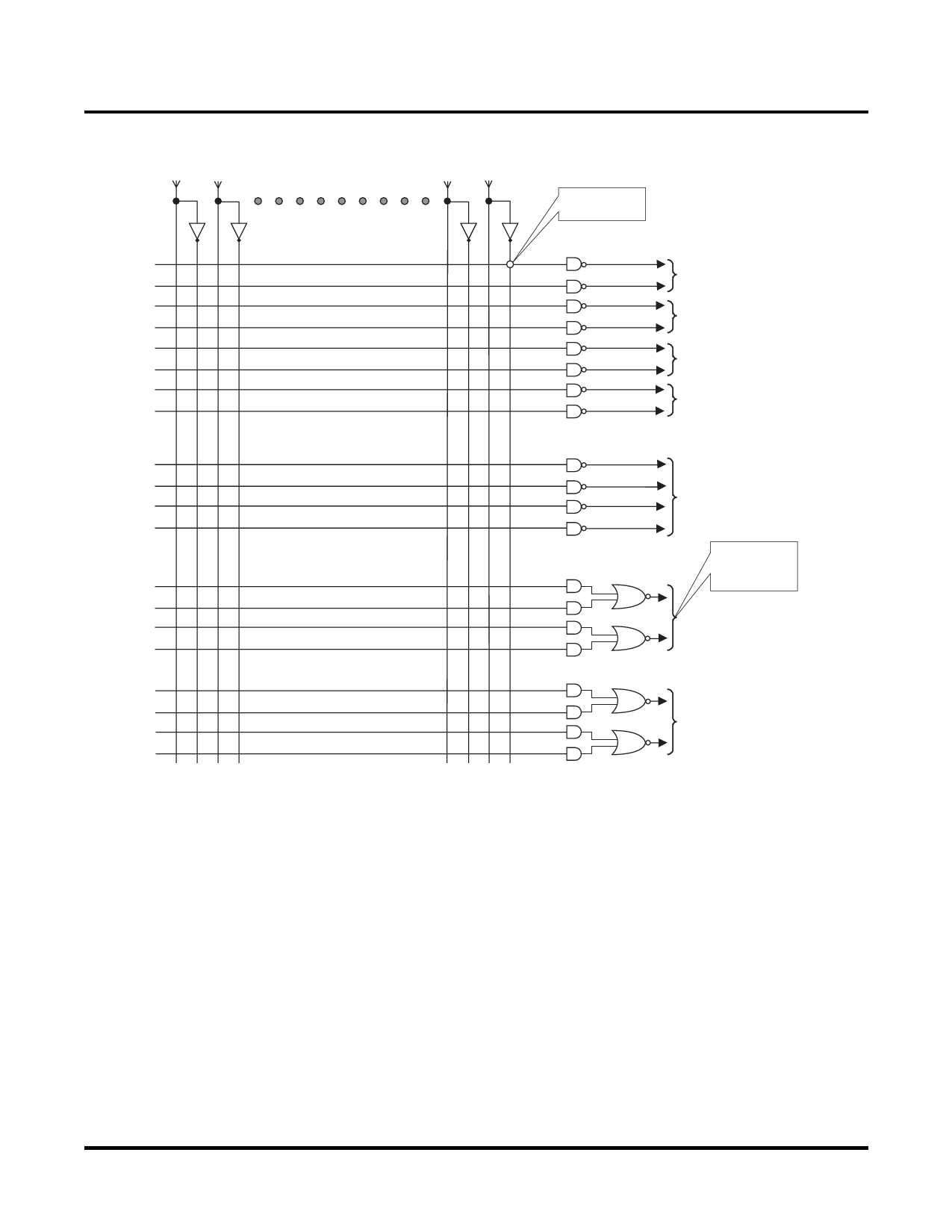
Figure 4. ispGDX2 Family Control Array
32 Inputs from Control GRP
ispGDX2 Family Data Sheet
Each connection
is programmable.
MUX Select
to Nibble 0
MUX Select
to Nibble 1
MUX Select
to Nibble 2
MUX Select
to Nibble 3
To MRB Clock/
Clock Enable
On selected blocks,
this signal can reset
the M Divider of the
PLL.
To MRB
Set/Reset
To MRB
Output Enable
sysIO Banks
The inputs and outputs of ispGDX2 devices are divided into eight sysIO banks, where each bank is capable of sup-
porting different I/O standards. The number of I/Os per bank is 32, 16 and 8 for the 256-, 128- and 64-I/O devices
respectively. Each sysIO bank has its own I/O supply voltage (VCCO) and reference voltage (VREF), allowing each
bank complete independence from the other banks. Each I/O within a bank can be individually configured to any
standard consistent with the VCCO and VREF settings. Figure 5 shows the I/O banks for the ispGDX2-256 device.
The I/O of the ispGDX2 devices contain a programmable strength and slew rate tri-state output buffer, a program-
mable input buffer, a programmable pull-up resistor, a programmable pull-down resistor and a programmable bus-
keeper latch. These programmable capabilities allow the support of a wide range of I/O standards.
7
Share Link: 