KA7525B データシートの表示(PDF) - Fairchild Semiconductor
部品番号
コンポーネント説明
メーカー
KA7525B Datasheet PDF : 18 Pages
| |||
KA7525B
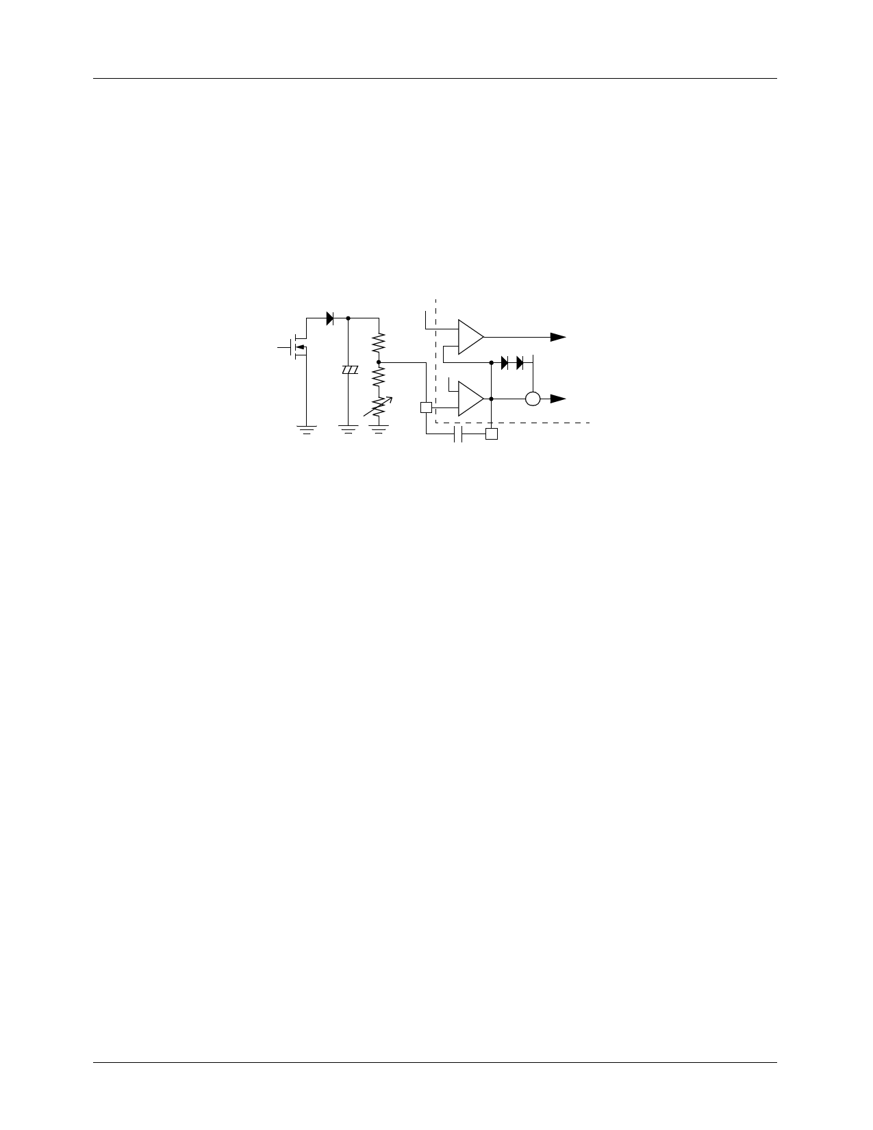
Error Amplifier
An Error Amplifier with access to the inverting input and output is provided. The noninverting input is internally biased at
2.5V and is not pinned out. The output voltage of the power factor converter is typically divided down and monitored by the
inverting input. The error amp output is internally connected to the multiplier and is pinned out for external loop compensa-
tion. Typically, the bandwidth is set below 20Hz, so that the amplifer’s output voltage is relatively constant over a given ac line
cycle. In effect, the error amp monitors the average output voltage of the converter over several line cycles. Input bias cur-
rent(0.5uA, max) can cause an output voltage error that is equal to the product of the input bias current and the value of the
upper divider resistor, R1 in Fig. 2.1.
1.8V
R1
+
R2
R3 1
INV
Band width= 1/(2π×R1×Ccomp)
Over Voltage
Comparator To Drive
+
Output Shutdown
-
Vref
Vref
+
-
D1 D2 _
+
+
To Multiplier
2
Ccomp EA OUT
Figure 2.1 Error Amp and Over Voltage Comparator
Over Voltage Protection
The low bandwidth (typically below 20Hz) characteristic of Error Amplifier control loop results in output voltage runaway
condition. This condition can occur during initial start-up, sudden load removal, or during output arcing. The over voltage
comparator monitors the output voltage of the error amplifier. When load is removed, error amp output swings lower than
1.8V, comparator is triggered high and output driver is turned off till the error amp inverting input voltage drops below 2.5V.
At this point, the error amp output swings positive, turns the output driver back on. The diode, D1,D2 clamp the error amp out-
put voltage to two diode drops above reference voltage. This prohibits the error amplifier from being saturated, allowing it to
recover faster thus minimizing the boost voltage overshoot.
Multiplier
A single quadrant, two input multiplier is the critical element that enables this device to get power factor correction. One input
of multiplier(Pin 3) is connected to an external resistor divider monitoring the rectified ac line. The other input is internally
driven by a DC voltage which is the difference of error amplifier output (Pin 2) and reference voltage, Vref. The multiplier is
designed to have an extremely linear transfer curve over a wide dynamic range, 0V to 2V for Pin 3, and 2.5V to 3.5V for the
error amplifier output under all line and load conditions.
The multiplier output controls the current sense comparator threshold as the ac voltage traverses sinusoidally from zero to
peak line. This allows the inductor peak current to follow the ac line thus forcing the average input current to be sinusoidal. In
other words, this has the effect of forcing the MOSFET on-time to track the input line voltage, resulting in a fixed drive output
on-time, thus making the preconverter load appear to be resistive to the ac line.
10
Share Link: 