KA7525B データシートの表示(PDF) - Fairchild Semiconductor
部品番号
コンポーネント説明
メーカー
KA7525B Datasheet PDF : 18 Pages
| |||
KA7525B
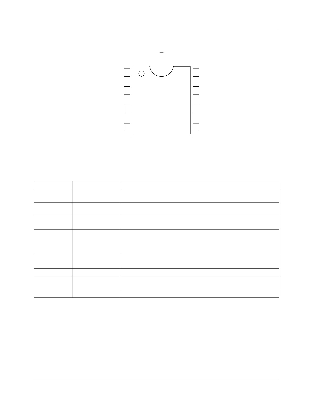
Pin Assignments
INV 1
EA OUT 2
MULT 3
CS 4
(Top View)
8 Vcc
7 OUT
6 GND
5 Idet
Pin Definitions
Pin Number
Pin Name
1
INV
2
EA_OUT
3
MULT
4
CS
5
Idet
6
GND
7
OUT
8
Vcc
Pin Function Description
Inverting input of the error amplifier. The output of the Boost converter
should be resistively divided to 2.5V and connected to this pin.
The output of the error amplifier. A feedback compensation network is
placed between this pin and the INV pin.
Input of the multiplier stage. The full-wave rectified AC is divided to less
than 2V and is connected to this pin.
Input of the PWM comparator. Current is sensed in the Boost stage
MOSFET by a resistor in the source lead. An internal leading edge
blanking circuitry has been included to reject any high frequency noise
present on the current waveform.
The zero current detector senses the inductor current by monitoring
when the Boost inductor auxiliary winding voltage falls below 1.8V.
The ground potential of all the pins.
The output of a high current power driver capable of driving the gate of a
power MOSFET.
The logic and control power supply connection.
2
Share Link: 