KS0072 データシートの表示(PDF) - Samsung
部品番号
コンポーネント説明
メーカー
KS0072 Datasheet PDF : 32 Pages
| |||
KS0072
PIN DESCRIPTION
PRELIMINARY SPECIFICATION
DOT MATRIX LCD CONTROLLER & DRIVER
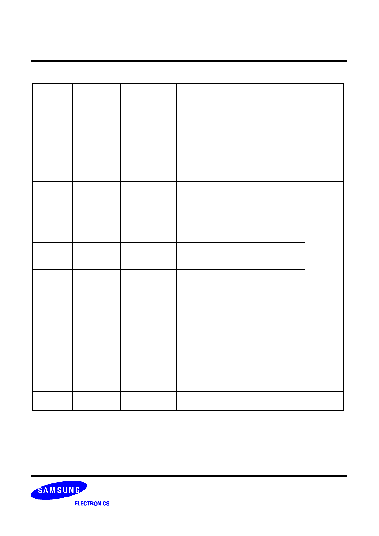
Pin
VDD
VSS(GND)
V2, V3, V5
S1 ~ S40
C1 ~ C16
Input/Output
Name
P
Power supply &
LCD Bias pin
Output
Output
Segment output
Common output
EXTCLK Input
External clock
Input
EXT_INT Input
RS
Input
External/Internal
oscillator clock
select
Register select
R/W
Input
Read/Write
E
Input
DB0 ~ DB3 Input/Output
Read/Write
enable
Data Bus 0 ~ 7
DB4 ~ DB7
RESETB Input
TEST
Output
Reset
Test Pin
Description
for logical circuit (+3v, +5v)
0V (GND)
Bias voltage level for LCD driving
Segment signal output for LCD driving
Common signal output for LCD driving
When using external clock, used as
clock input pin. When using internal
oscillator, connect to VDD or VSS.
When EXT_INT = “High”, external clock
is used. When “Low”, internal oscillator is
used.
Used as register selection input. When
RS= “High”, Data register is selected.
When RS= “Low”, Instruction register is
selected.
Used as read/write selection input. When
RW=“High”,read operation. When
RW=“Low”, write operation.
Used as read/write enable signal.
When 8-bit bus mode, used as low order
bidirectional data bus.
During 4-bit bus mode open these pins.
When 8-bit bus mode, used as high order
bidirectional data bus. IN case of 4-bit
bus mode, used as both high and low
order.
DB7 is used for Busy Flag output during
read instruction operation.
If it is necessary to initialize the system
by hardware, force “Low”, level signal to
this terminal about 1.2 mS.
Internal oscillator test pin.
Openthis pin.
Interface
Power
Supply
LCD
LCD
External
clock
MPU
MPU
LDI-97-D001
5
97-10-23
Share Link: 