KS8001L データシートの表示(PDF) - Micrel
部品番号
コンポーネント説明
メーカー
KS8001L Datasheet PDF : 46 Pages
| |||
Micrel
KSZ8001
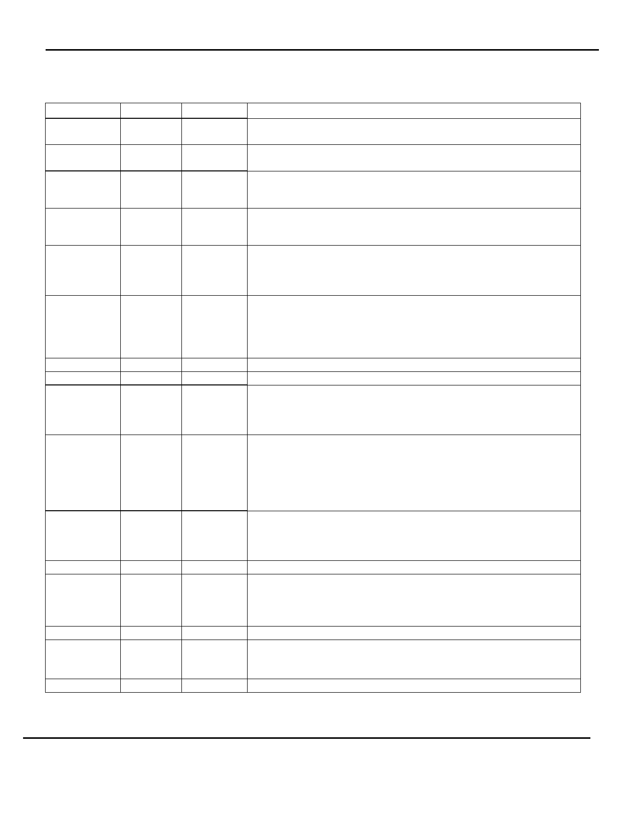
Pin Description
Pin Number
1
2
3
4
5
6
7
8
9
10
11
12
13
14
15
16
Pin Name
MDIO
Type (Note 1)
I/O
MDC
I
RXD3/
PHYAD1
RXD2/
PHYAD2
Ipd/O
Ipd/O
RXD1/
RXD[1]/
PHYAD3
Ipd/O
RXD0/
RXD[0]/
RX
PHYAD4
Ipd/O
VDDIO
GND
RXDV/
CRSDV/
PCS_LPBK
Pwr
Gnd
Ipd/O
RXC/
SMII_SELE
CT
Ipd/O
RXER/
RX_ER/
ISO
GND
VDDC
Ipd/O
Gnd
Pwr
TXER
Ipd
TXC/
I/O
REFCLK/
CLOCK
TXEN
Ipd
Pin Function
MII Management (MIIM) Interface: Data I/O
This pin requires an external 4.7K pull-up resistor.
MII Management (MIIM) Interface: Clock Input
This pin is synchronous to the MDIO data line.
MII Mode: Receive Data Output[3]2 /
Configuration Mode: The pull-up/pull-down value is latched as PHYADDR[1]
during reset. See “Strapping Options” section for details.
MII Mode: MII Receive Data Output[2]2 /
Configuration Mode: The pull-up/pull-down value is latched as PHYADDR[2]
during reset. See “Strapping Options” section for details.
MII Mode: Receive Data Output[1]2 /
RMII Mode: Receive Data Output[1]3 /
Configuration Mode: The pull-up/pull-down value is latched as PHYADDR[3]
during reset. See “Strapping Options” section for details.
MII Mode: Receive Data Output[0]2 /
RMII Mode: Receive Data Output[0]3 /
SMII Mode: Receive Data and Control4 /
Configuration Mode: The pull-up/pull-down value is latched as PHYADDR[4]
during reset. See “Strapping Options” section for details.
3.3V digital VDD
Ground
MII Mode: Receive Data Valid Output /
RMII Mode: Carrier Sense/Receive Data Valid /
Configuration Mode: The pull-up/pull-down value is latched as pcs_lpbk
during reset. See “Strapping Options” section for details.
MII Receive Clock Output
Operating at:
25 MHz = 100 Mbps
2.5 MHz = 10 Mbps
Configuration Mode: The pull-up/pull-down value is latched as SMII during
reset. See “Strapping Options” section for details.
MII Mode: Receive Error Output /
RMII Mode: Receive Error /
Configuration Mode: The pull-up/pull-down value is latched as ISOLATE
during reset. See “Strapping Options” section for details.
Ground
1.8V digital core VDD
VDD output
:
KSZ8001L / KSZ8001SL
VDD input
:
KSZ8001S
(See “Circuit Design Reference for Power Supply” section for details)
MII Transmit Error Input
MII Mode: MII Transmit Clock Output /
RMII Mode: 50 MHz Reference Clock Input /
SMII Mode: 125 MHz Synchronization Clock Input
MII Transmit Enable Input
June 2009
Revision 1.04
6
Share Link: 