L6910(2003) データシートの表示(PDF) - STMicroelectronics
部品番号
コンポーネント説明
メーカー
L6910 Datasheet PDF : 21 Pages
| |||
L6910A L6910
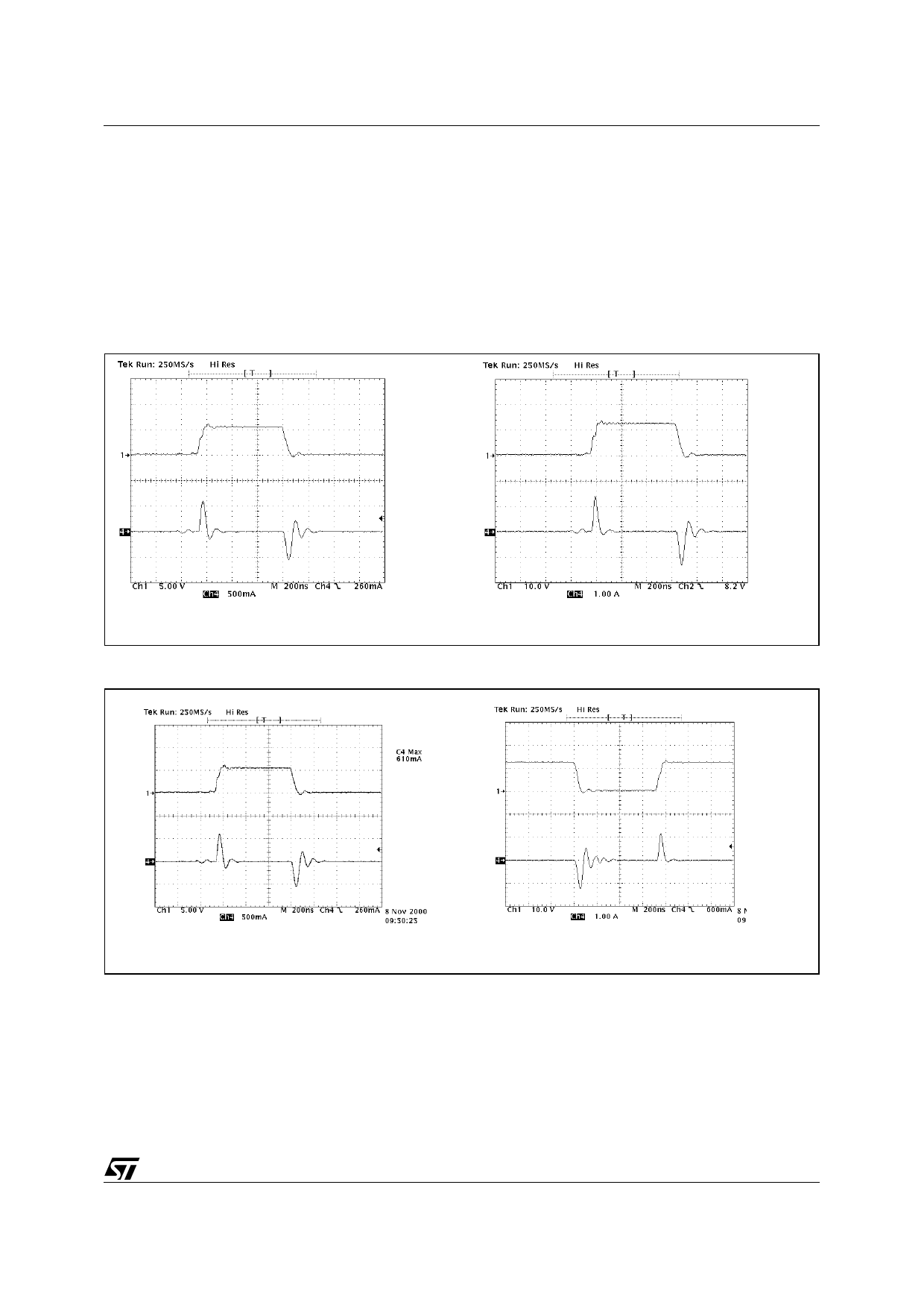
Figure 3. High Side driver peak current. Vboot-Vphase = 12V (right) Vboot-Vphase = 5V (left)
CH1 = High Side Gate CH4 = Gate Current
Figure 4. Low Side driver peak current. VCC = 12V (right) VCC = 5V (left)
CH1 = Low Side Gate CH4 = Gate Current
Monitoring and Protections
The output voltage is monitored by means of pin FB. If it is not within ±10% (typ.) of the programmed value, the
powergood output is forced low.
The device provides overvoltage protection, when the voltage sensed on pin FB reaches a value 17% (typ.)
greater than the reference the OSC pin is forced high (3V typ.) and the lower driver is turned on as long as the
over-voltage is detected.
Overcurrent protection is performed by the device comparing the drop across the high side MOS, due to the
RDSON, with the voltage across the external resistor (ROCS) connected between the OCSET pin and drain of the
upper MOS. Thus the overcurrent threshold (IP) can be calculated with the following relationship:
IP = R-----O---R-C----dS---s--⋅-O--I--ON----C----S-
Where the typical value of IOCS is 200µA. To calculate the ROCS value it must be considered the maximum
RdsON (also the variation with temperature) and the minimum value of IOCS. To avoid undesirable trigger of
overcurrent protection this relationship must be satisfied:
7/21
Share Link: 