L6910 データシートの表示(PDF) - STMicroelectronics
部品番号
コンポーネント説明
メーカー
L6910 Datasheet PDF : 29 Pages
| |||
L6910 - L6910A
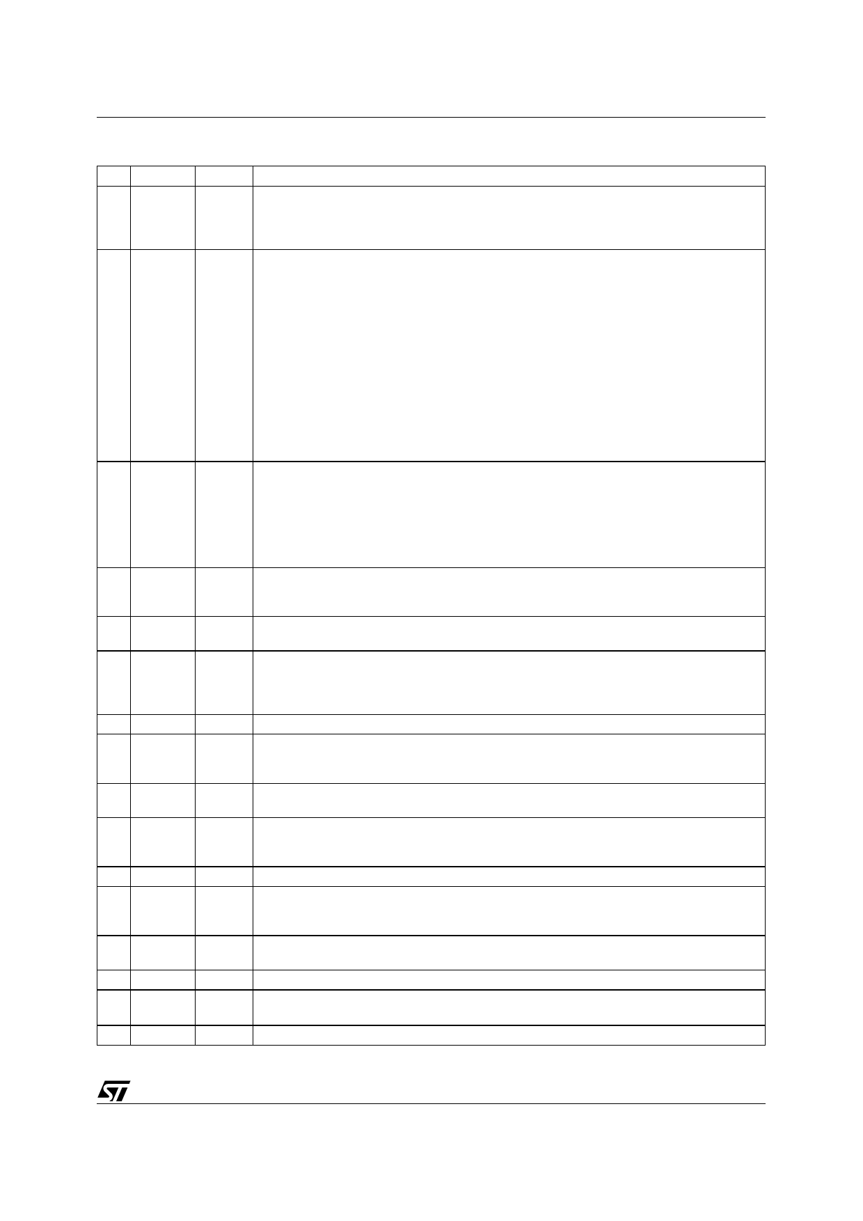
Table 4. Pins Function
SO HTSSOP Name
Description
1
1
VREF Internal 0.9V ±1.5% reference is available for external regulators or for the internal error
amplifier (connecting this pin to EAREF) if external reference is not available.
A minimum 1nF capacitor is required.
If the pin is forced to a voltage lower than 70%, the device enters the hiccup mode.
2
2
OSC Oscillator switching frequency pin. Connecting an external resistor (RT) from this pin to
GND, the external frequency is increased according to the equation:
f O S C ,RT
=
200KHz + -4---.-9----4-----⋅---1---0----6-
RT(KΩ)
Connecting a resistor (RT) from this pin to Vcc (12V), the switching frequency is reduced
according to the equation:
f O S C ,RT
=
200KHz – 4----.-3----0---6-----⋅---1---0----7-
RT(KΩ)
If the pin is not connected, the switching frequency is 200KHz.
The voltage at this pin is fixed at 1.23V. Forcing a 50µA current into this pin, the built in
oscillator stops to switch.
In Over Voltage condition this pin goes over 3V until that conditon is removed.
3
3
OCSET A resistor connected from this pin and the upper Mos Drain sets the current limit
protection.
The internal 200µA current generator sinks a constant current through the external
resistor. The Over-Current threshold is due to the following equation:
IP
=
I--O----C----S----E---T-----⋅---R----O----C----S----E---T-
RDSon
4
4
SS/INH The soft start time is programmed connecting an external capacitor from this pin and
GND. The internal current generator forces through the capacitor 10µA.
This pin can be used to disable the device forcing a voltage lower than 0.4V
5
6
COMP This pin is connected to the error amplifier output and is used to compensate the voltage
control feedback loop.
6
7
FB This pin is connected to the error amplifier inverting input and is used to compensate the
voltage control feedback loop.
Connected to the output resistor divider, if used, or directly to Vout, it manages also over-
voltage conditions and the PGOOD signal
7
8
GND All the internal references are referred to this pin. Connect it to the PCB signal ground.
8
9
EAREF Error amplifier non-inverting input. Connect to this pin an external reference (from 0.9V to
3V) for the PWM regulation or short it to VREF pin to use the internal reference.
If this pin goes under 650mV (typ), the device shuts down.
9
10
PGOOD This pin is an open collector output and it is pulled low if the output voltage is not within the
above specified thresholds. If not used it may be left floating.
10
11
PHASE This pin is connected to the source of the upper mosfet and provides the return path for the
high side driver. This pin monitors the drop across the upper mosfet for the current limit
together with OCSET.
11
12
HGATE High side gate driver output.
12
13
BOOT Bootstrap capacitor pin. Through this pin is supplied the high side driver and the upper
mosfet. Connect through a capacitor to the PHASE pin and through a diode to Vcc
(cathode vs. boot).
13
14
PGND Power ground pin. This pin has to be connected closely to the low side mosfet source in
order to reduce the noise injection into the device
14
5
LGATE This pin is the lower mosfet gate driver output
15
16
16
5
VCC
N.C.
Device supply voltage. The operative supply voltage ranges is from 5V to 12V.
DO NOT CONNECT VIN TO A VOLTAGE GREATER THAN VCC.
This pin is not internally bonded. It may be left floating or connected to GND.
3/29
Share Link: 