L6910 データシートの表示(PDF) - STMicroelectronics
部品番号
コンポーネント説明
メーカー
L6910 Datasheet PDF : 29 Pages
| |||
L6910 - L6910A
4 DEVICE DESCRIPTION
The device is an integrated circuit realized in BCD technology. The controller provides complete con-
trol logic and protection for a high performance step-down DC-DC converter. It is designed to drive N
Channel Mosfets in a synchronous-rectified buck topology. The output voltage of the converter can be
precisely regulated down to 900mV with a maximum tolerance of ±1.5% when the internal reference is
used (simply connecting together EAREF and VREF pins). The device allows also using an external
reference (0.9V to 3V) for the regulation. The device provides voltage-mode control with fast transient
response. It includes a 200kHz free-running oscillator that is adjustable from 50kHz to 1MHz. The er-
ror amplifier features a 10MHz gain-bandwidth product and 10V/µs slew rate that permits to realize
high converter bandwidth for fast transient performance. The PWM duty cycle can range from 0% to
100%. The device protects against over-current conditions entering in HICCUP mode. The device
monitors the current by using the rDS(ON) of the upper MOSFET(s) that eliminates the need for a cur-
rent sensing resistor. The device is available in SO16 narrow package.
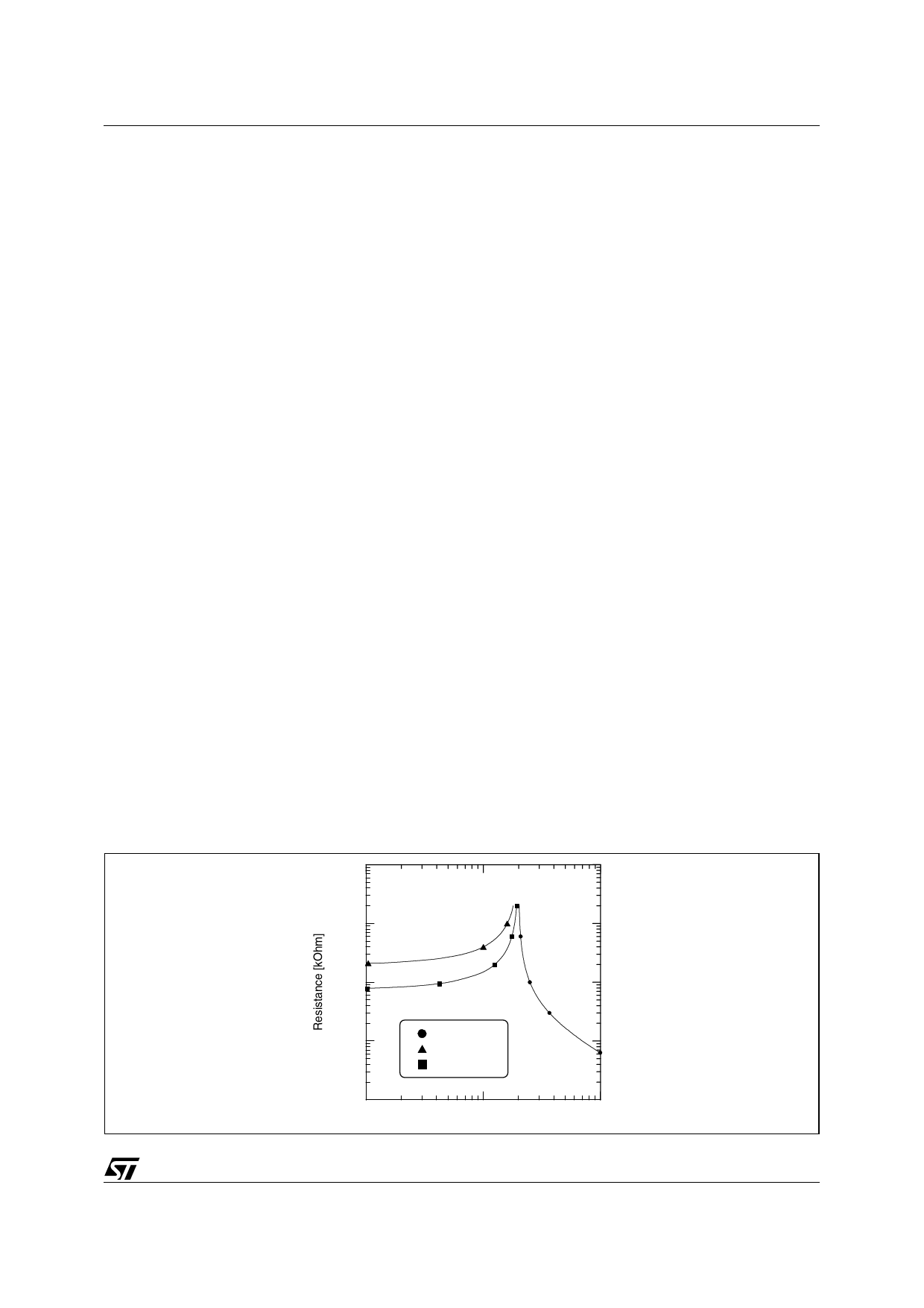
4.1 Oscillator
The switching frequency is internally fixed to 200kHz. The internal oscillator generates the triangular waveform
for the PWM charging and discharging with a constant current an internal capacitor. The current delivered to the
oscillator is typically 50µA (Fsw = 200KHz) and may be varied using an external resistor (RT) connected between
OSC pin and GND or VCC. Since the OSC pin is maintained at fixed voltage (typ. 1.235V), the frequency is var-
ied proportionally to the current sunk (forced) from (into) the pin.
In particular connecting RT vs. GND the frequency is increased (current is sunk from the pin), according to the
following relationship:
f O S C ,RT
=
200KHz + 4----.-9----4-----⋅---1---0----6-
RT(KΩ)
Connecting RT to VCC = 12V or to VCC = 5V the frequency is reduced (current is forced into the pin), according
to the following relationships:
fO S C ,RT
=
200KHz – -4---.--3---0---6-----⋅---1---0----7-
RT(KΩ)
VCC = 12V
fOSC,RT = 200KHz – R-1---5-T---(-⋅--K-1---Ω0----6-)-
VCC = 5V
Switching frequency variation vs. RT are repeated in Fig. 4.
Note that forcing a 50µA current into this pin, the device stops switching because no current is delivered to the
oscillator.
Figure 4.
10000
1000
100
10
10
RT to GND
RT to VCC=12V
RT to VCC=5V
100
Frequency [kHz]
1000
5/29
Share Link: 