L6910G データシートの表示(PDF) - STMicroelectronics
部品番号
コンポーネント説明
メーカー
L6910G Datasheet PDF : 26 Pages
| |||
L6910G
4.2 Reference
A precise ±1.5% 0.9V reference is available. This reference must be filtered with 1nF ceramic capacitor to avoid
instability in the internal linear regulator. It is able to deliver up to 100µA and may be used as reference for the
device regulation and also for other devices. If forced under 70% of its nominal value, the device enters in Hic-
cup mode until this condition is removed.
Through the EAREF pin the reference for the regulation is taken. This pin directly connects the non-inverting
input of the error amplifier. An external reference (or the internal 0.9V ±1.5%) may be used. The input for this
pin can range from 0.9V to 3V. It has an internal pull-down (300kΩ resistor) that forces the device shutdown if
no reference is connected (pin floating). However the device is shut down if the voltage on the EAREF pin is
lower than 650mV (typ).
4.3 Soft Start
At start-up a ramp is generated charging the external capacitor CSS with an internal current generator. The initial
value for this current is of 35µA and speeds-up the charge of the capacitor up to 0.5V. After that it becames
10µA until the final charge value of approximatively 4V.
When the voltage across the soft start capacitor (VSS) reaches 0.5V the lower power MOS is turned on to dis-
charge the output capacitor. As VSS reaches 1.1V (i.e. the oscillator triangular wave inferior limit) also the upper
MOS begins to switch and the output voltage starts to increase.
No switching activity is observable if SS is kept lower than 0.5V and both mosfets are off.
If VCC and OCSET pins are not above their own turn-on thresholds and VEAREF is not above 650mV, the Soft-
Start will not take place, and the relative pin is internally shorted to GND. During normal operation, if any under-
voltage is detected on one of the two supplies, the SS pin is internally shorted to GND and so the SS capacitor
is rapidly discharged.
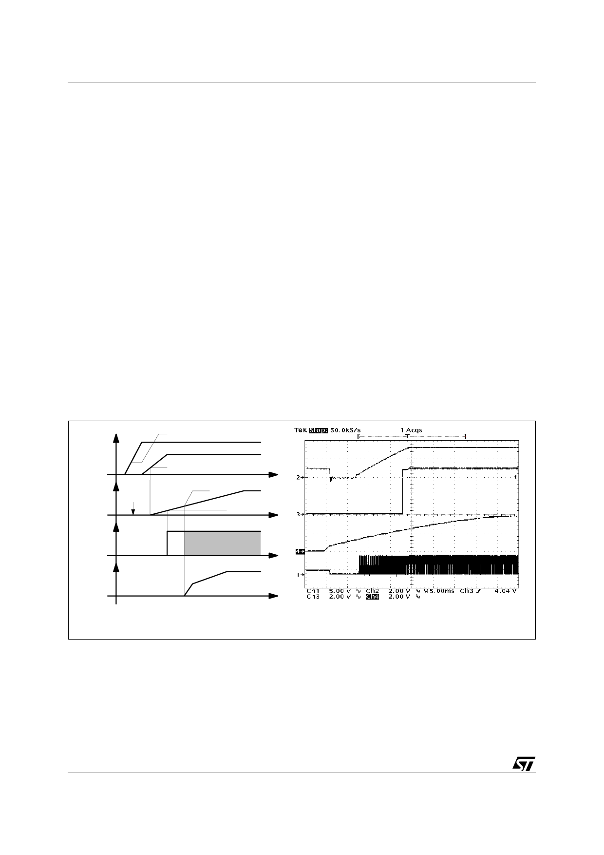
Figure 5. Soft Start (with Reference Present)
Vcc
Vin
Vcc Turn-on threshold
Vin Turn-on threshold
Vss
to GND
1V
0.5V
LGATE
Vout
Timing Diagram
Acquisition: CH1 = PHASE; CH2 = Vout;
CH3 = PGOOD; CH4 = Vss
4.4 Driver Section
The driver capability on the high and low side drivers allows using different types of power MOS (also multiple
MOS to reduce the RDSON), maintaining fast switching transition.
The low-side mos driver is supplied directly by Vcc while the high-side driver is supplied by the BOOT pin.
Adaptative dead time control is implemented to prevent cross-conduction and allow to use several kinds of mos-
fets. The upper mos turn-on is avoided if the lower gate is over about 200mV while the lower mos turn-on is
6/26
Share Link: 