LA75691 データシートの表示(PDF) - SANYO -> Panasonic
部品番号
コンポーネント説明
メーカー
LA75691 Datasheet PDF : 13 Pages
| |||
LA75691
Continued from preceding page.
Pin No.
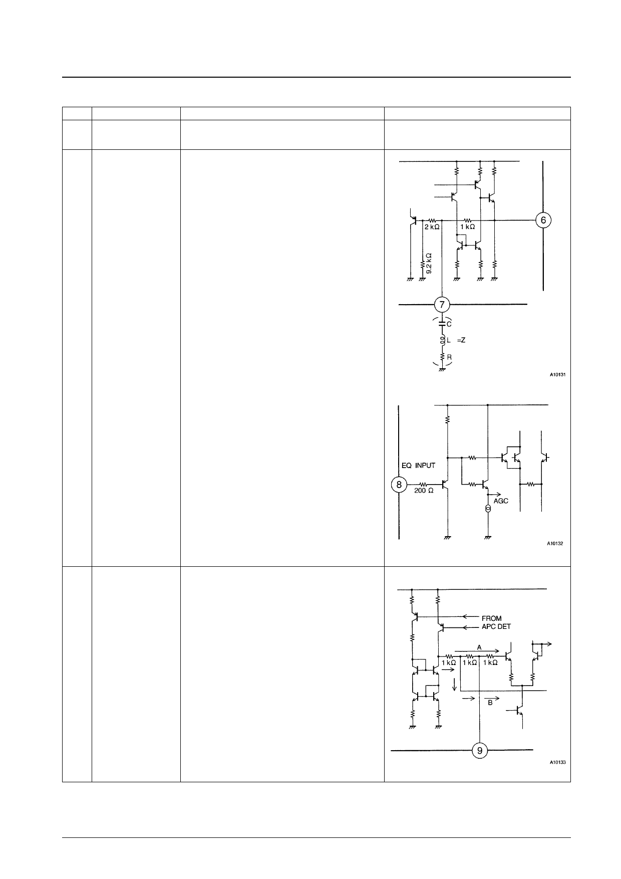
5
Pin
VCC
Function
The VCC to ground decoupling capacitors must be placed as
close to the IC as possible.
Equalizer circuit. This circuit corrects the frequency
characteristics of the video signal.
Pin 17 is the equalizer amplifier input. A 1.5-V p-p signal is
input to pin 17, and that signal is amplified to be a 2-V p-p
signal by the equalizer amplifier.
Equalizer amplifier design:
The equalizer amplifier is designed as a voltage-follower
amplifier with a gain of about 2.3 dB. Connect an inductor, a
capacitor, and a resistor in series between pin 7 and ground
if the frequency characteristics require correction.
Notes on the equalizer amplifier:
If the input signal is vi and the output signal is vo, then:
6
R1
7
EQ amp
—— +1 (vi + vin) = Vo × G
Z
8
G: The voltage-follower amplifier gain.
vin: Imaginary short
G: About 2.3 dB
Assuming that vin is 0, then:
VoG R1
AV = ——— = —— +1
Vi
Z
R1 is the IC internal resistance of 1 kΩ. Simply select Z to
match the desired characteristics. However, note that Z must
be chosen carefully in order not to cause distortion, since the
equalizer amplifier gain will be maximum at the resonance
determined by Z.
Equivalent circuit
PLL detector APC filter
The APC time constant is switched internally in the IC. When
locked, the VCO is controlled by loop A, and the gain is
reduced. When unlocked and in weak field reception, the
9
APC FILTER
VCO is controlled by loop B, and the gain is increased.
For this APC filter the recommended values are:
R should be between 150 and 390 Ω.
C should be 0.47 µF.
Continued on next page.
No. 5734-8/13
Share Link: 