LB11872H データシートの表示(PDF) - SANYO -> Panasonic
部品番号
コンポーネント説明
メーカー
LB11872H Datasheet PDF : 11 Pages
| |||
LB11872H
Pin Functions
Pin No.
2
3
4
5
6
7
Pin name
IN2+
IN2-
IN1+
IN1-
IN3+
IN3-
Function
Hall effect sensor signal inputs.
These inputs are high when IN+ is greater than
IN- and low when IN- is greater than IN+.
Insert capacitors between the IN+ and IN– pins to
reduce noise.
An amplitude of over 50mVp-p and under
350mVp-p is desirable for the Hall input signals.
Kickback can occur in the output waveform if the
Hall input amplitude is over 350mVp-p.
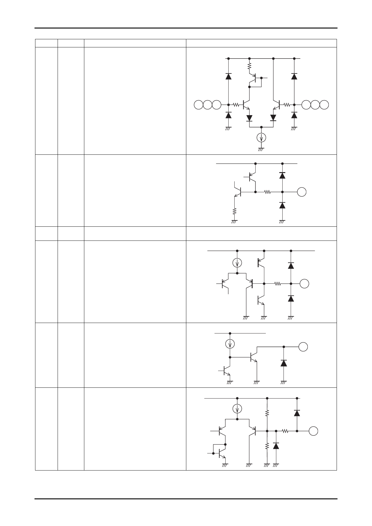
357
Equivalent circuit
VCC
300Ω
300Ω
246
8
AGC
AGC amplifier frequency characteristics
correction.
Insert a capacitor (about 0.022μF) between this
pin and ground.
VREG
300Ω
8
9
MN
Monitor pin.
This pin should be left open in normal operation.
12
CSD
Used for both initial reset pulse generation and as
the reference time for constraint protection
circuits.
Insert a capacitor between this pin and ground.
VREG
300Ω
12
14
FG
FG pulse output.
This is an open-collector output.
VREG
14
15
S/S
Start/stop control.
Low : Start 0 to 1.0V
High : Stop 2.0V to VREG
This pin goes to the high level when open.
VREG
33kΩ
5kΩ
15
30kΩ
Continued on next page.
No.7257-6/11
Share Link: 