LB11921T データシートの表示(PDF) - SANYO -> Panasonic
部品番号
コンポーネント説明
メーカー
LB11921T Datasheet PDF : 18 Pages
| |||
LB11921T
Continued from preceding page.
Pin No.
Symbol
Pin Description
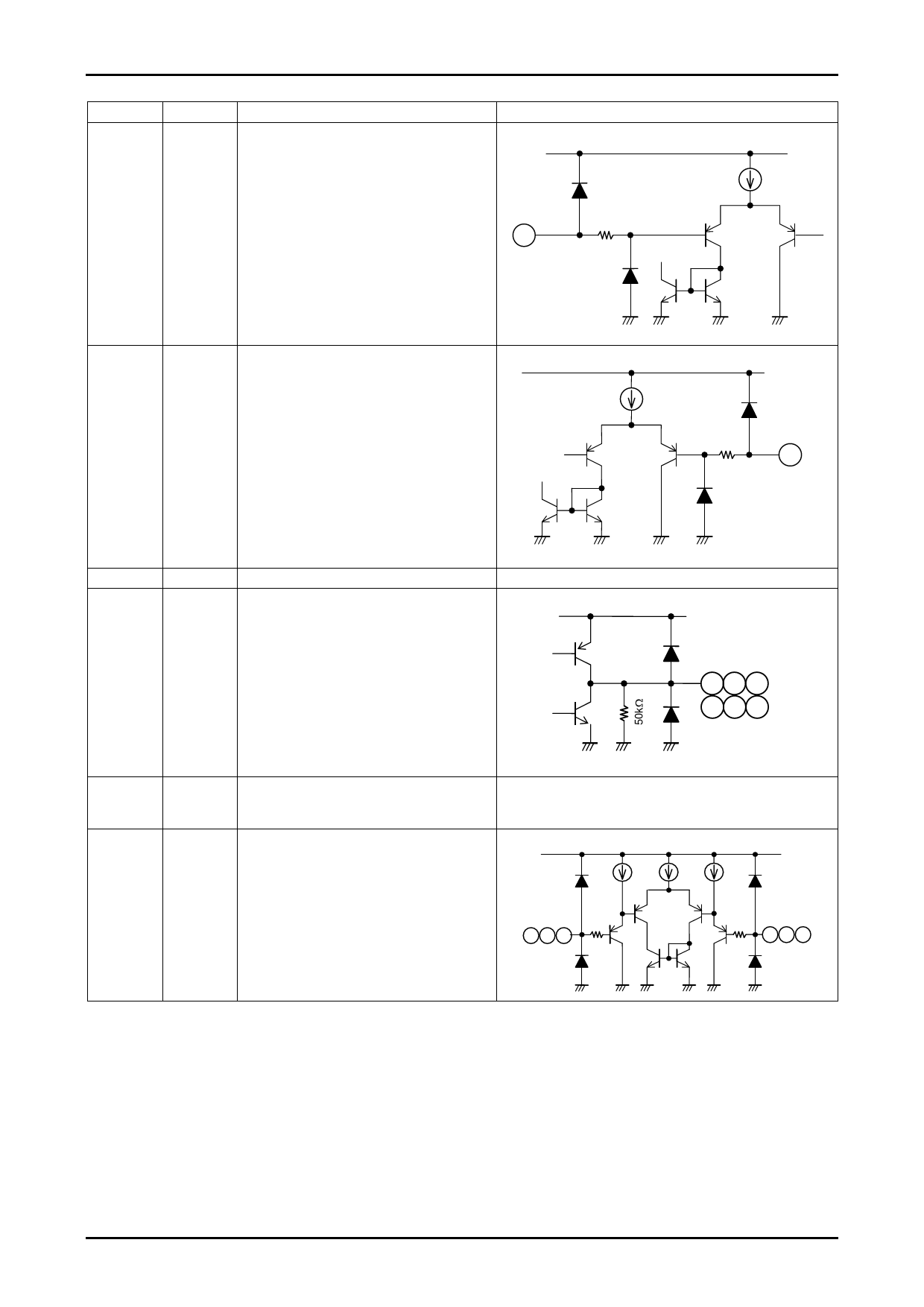
21
RF GND Output current detection reference
Connect to GND of the external resistor Rf.
VCC
Equivalent Circuit
21
22
RF
Output current detection
Connect a low resistance resistor Rf between this
VCC
pin and Rf GMD pin.
This resistor sets the maximum output current
IOUT to be 0.26/Rf.
22
23
GND
GND pin
24
UL
Outputs (that are used to drive external
25
UH
transistors).
26
VL
Duty cycle is controlled on the UH, VH, and WH
27
VH
side of these output.
28
WL
29
WH
VCC
30
VCC
Power supply
Connect a capacitor between this pin and ground
for stabilization.
31
IN3-
Hall-effect device inputs.
32
IN3+
The input is seen as a high-level input when IN+
VCC
33
IN2-
> IN-, and as a low-level input for the opposite
34
IN2+
state.
35
IN1-
If noise on the Hall-effect device signals is a
36
IN1+
problem, insert capacitors between the
corresponding IN+ and IN- inputs.
500Ω
32 34 36
24 26 28
25 27 29
500Ω
31 33 35
No.A0604-11/18
Share Link: 