LB11967V(2016) データシートの表示(PDF) - ON Semiconductor
部品番号
コンポーネント説明
メーカー
LB11967V Datasheet PDF : 10 Pages
| |||
LB11967V
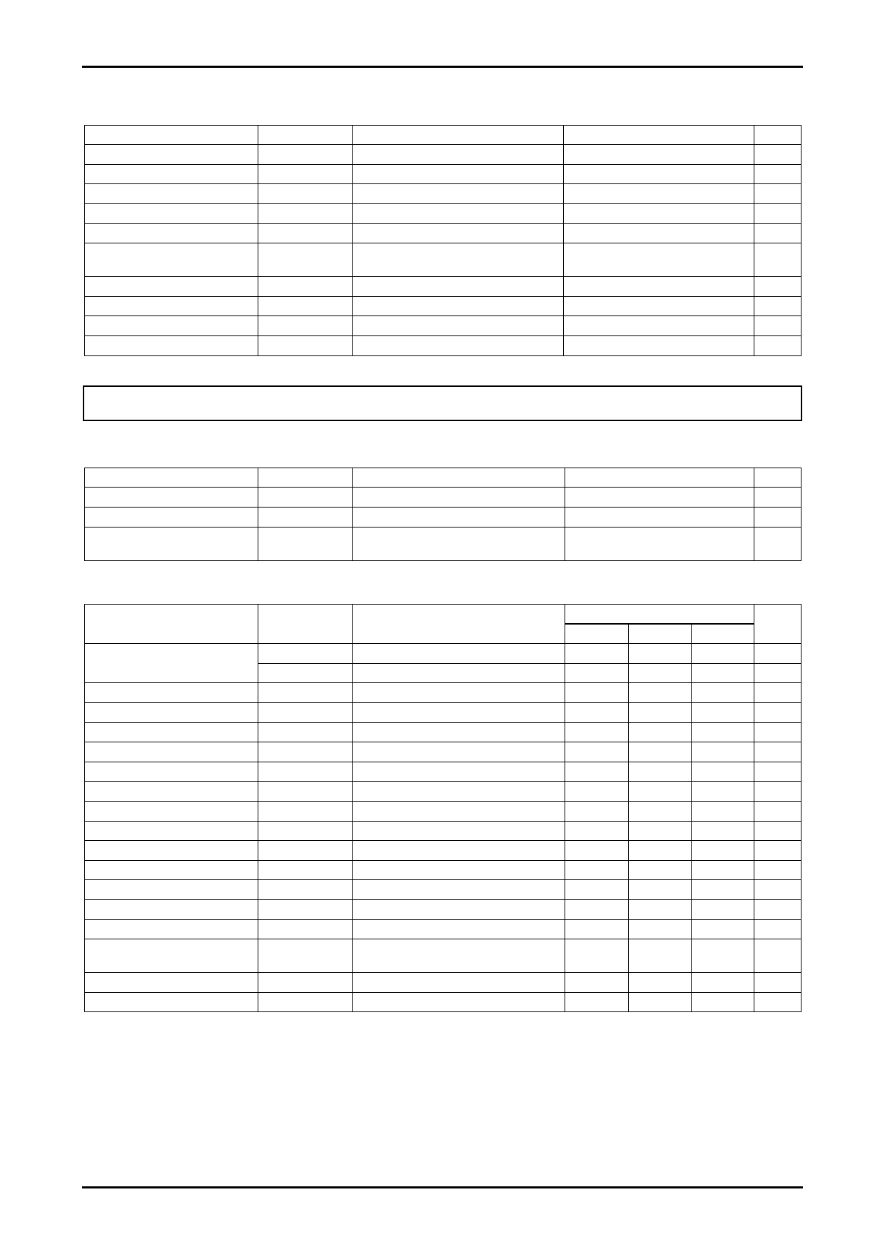
Specifications
Maximum Ratings at Ta = 25C (Note1)
Parameter
Symbol
Conditions
Ratings
Unit
VCC maximum supply voltage
OUT pin maximum output current
OUT pin output withstand voltage
HB maximum output current
VTH input pin withstand voltage
RD/FG output pin output
withstand voltage
VCC max
IOUT max
VOUT max
IHB max
VVTH max
VRD/VFG max
18
V
50 mA
18
V
10 mA
8
V
18
V
RD/FG output current
Allowable power dissipation
IRD/IFG max
Pd max
Mounted on a specified board (Note2)
10 mA
800 mW
Operating temperature range
Topr
-30 to +95
C
Storage temperature range
Tstg
-55 to +150
C
1. Stresses exceeding those listed in the Maximum Rating table may damage the device. If any of these limits are exceeded, device functionality should not be
assumed, damage may occur and reliability may be affected.
2. Specified board: 114.3mm × 76.1mm × 1.6mm, glass epoxy board.
Recommended Operating Conditions at Ta = 25C (Note3)
Parameter
Symbol
Conditions
Ratings
Unit
VCC supply voltage
VTH input level voltage range
VCC
VTH
Full speed mode
6 to 16
V
0 to 7
V
Hall input common phase input
VICM
0.2 to 3
V
voltage range
3. Functional operation above the stresses listed in the Recommended Operating Ranges is not implied. Extended exposure to stresses beyond the
Recommended Operating Ranges limits may affect device reliability.
Electrical Characteristics at Ta = 25C, VCC = 12V, unless otherwise specified. (Note4)
Parameter
Symbol
Conditions
Ratings
Unit
min
typ
max
Circuit current
6VREG voltage
HB voltage
VOVER voltage
CPWM-H level voltage
CPWM-L level voltage
CPWM oscillation frequency
ICC1
ICC2
6VREG
VHB
VVOVER
VCRH
VCRL
FPWM
During drive
During lock protection
I6VREG = 5mA
IHB = 5mA
IVOVER = 1mA
C = 100pF
6
10
14 mA
6
10
14 mA
5.80
6.0
6.15
V
1.05
1.22
1.35
V
12.0
12.8
13.6
V
4.35
4.55
4.75
V
1.45
1.65
1.85
V
18
25
32 kHz
CT pin H level voltage
VCTH
3.4
3.6
3.8
V
CT pin L level voltage
VCTL
1.4
1.6
1.8
V
ICT pin charge current
ICT1
VCT = 1.2V
1.6
2.0
2.5 A
ICT pin discharge current
ICT2
VCT = 4.0V
0.16
0.20
0.28 A
ICT charge/discharge current ratio
RCT
ICT1/ICT2
8
10
12 deg
OUT-N output voltage
VON
IO = 20mA
4
10
V
OUT-P sink current
IOP
15
20
mA
Hall input sensitivity
VHN
Zero peak value
10
20 mV
(including offset and hysteresis)
RD/FG output pin L voltage
VRD/VFG
IRD/IFG = 5mA
0.15
0.3
V
RD/FG output pin leak current
IRDL/IFGL
VRD/VFG = 16V
30 A
4. Product parametric performance is indicated in the Electrical Characteristics for the listed test conditions, unless otherwise noted. Product performance may
not be indicated by the Electrical Characteristics if operated under different conditions.
www.onsemi.com
2
Share Link: 