LB1980JH データシートの表示(PDF) - SANYO -> Panasonic
部品番号
コンポーネント説明
メーカー
LB1980JH Datasheet PDF : 7 Pages
| |||
LB1980JH
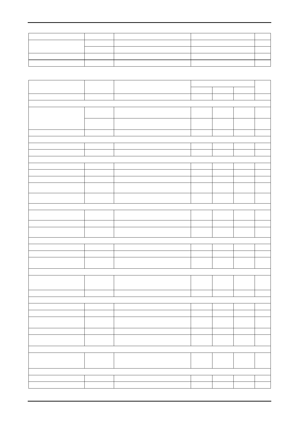
Allowable Operating Ranges at Ta = 25°C
Parameter
Supply voltage
Hall input amplitude
GSENSE pin input range
Symbol
VS
VCC
VHALL
VGSENSE
Conditions
Between the hall inputs
With respect to the control system ground
Ratings
5 to 22
4.5 to 5.5
±30 to ±80
-0.20 to +0.20
Unit
V
V
mVo-p
V
Electrical Characteristics at Ta = 25°C, VCC = 5V,VS = 15V
Parameter
Symbol
Conditions
VCC supply current
Outputs
ICC
RL=∞, VCTL=0V, VLIM=0V (Quiescent)
Output saturation voltage
Output leakage current
FR
VO sat1
VO sat2
IO leak
IO=500mA, Rf=0.5Ω, Sink+Source
VCTL=VLIM=5V(With saturation prevention)
IO=1.0mA, Rf=0.5Ω, Sink+Source
VCTL=VLIM=5V(With saturation prevention)
FR pin input threshold voltage
FR pin input bias current
Control
VFSR
IB(FSR)
CTLREF pin voltage
CTLREF pin input range
CTL pin input bias current
CTL pin control start voltage
CTL pin control Gm
Current Limiter
VCREF
VCREFIN
IB(CTL)
VCTL(ST)
Gm(CTL)
With VCTL=5V and the CTLREF pin open
With Rf=0.5Ω, VLIM=5V, IO≥10mA,
Hall input logic fixed (U, V, W=H, H, L)
With Rf=0.5Ω, ∆IO=200mA,
Hall input logic fixed (U, V, W=H, H, L)
LIM current limit offset voltage
LIM pin input bias current
LIM pin current control level
Hall Amplifier
Voff(LIM)
IB(LIM)
ILIM
With Rf=0.5Ω, VCTL=5V, IO≥10mA,
Hall input logic fixed (U, V, W=H, H, L)
With VCTL=5V and the VCREF pin open
With Rf=0.5Ω, VCTL=5V, VLIM=2.06V
Hall input logic fixed (U, V, W=H, H, L)
Hall amplifier input offset voltage Voff(HALL)
Hall amplifier input bias current
Hall amplifier common-mode
input voltage range
TRC
IB(HALL)
VCM(HALL)
Torque ripple correction ratio
ADJ pin voltage
FG Amplifier
TRC
VADJ
For the high and low peaks in the
Rf waveform when IO=200mA.
(Rf=0.5Ω, with the ADJ pin open) *1
FG amplifier input offset voltage
Voff(FG)
FG amplifier input bias current
FG amplifier output saturation
voltage
FG amplifier voltage gain
FG amplifier common-mode
input voltage
Saturation
IB(FG)
VO sat (FG)
VG(FG)
VGM(FG)
Sink side, for the load provided by the internal
pull-up resistor
For the open loop state with f=10kHz
Saturation prevention circuit
lower side voltage setting
TSD
VO sat(DET)
The voltages between each OUT and
Rf pair when IO=10mA, Rf=0.5Ω, and
VCTL=VLIM=5V
TSD operating temperature
TSD
Design target value *2
Hysteresis width
∆TSD
Design target value *2
Notes : *1. The torque ripple correction ratio is determined as follows from the Rf voltage waveform.
*2. Parameters that are indicated as design target values in the conditions column are not tested.
min
2.25
-5.0
2.05
1.50
2.00
0.46
140
-2.5
830
-6
2.37
-8
-100
41.5
0.5
0.175
Ratings
typ
12
2.1
2.6
2.50
2.15
2.15
0.58
200
900
1.0
1.3
9
2.50
44.5
0.25
180
20
Unit
max
18 mA
2.6
V
3.5
V
1.0 mA
2.75
V
mA
2.25
V
3.50
V
4.0 µA
2.30
V
0.70 A / V
260 mV
µA
970 mA
+6 mA
3.0 µA
3.3
V
%
2.63
V
+8 mV
nA
0.5
V
47.5 dB
4.0
V
0.325
V
°C
°C
No.A0231-2/7
Share Link: 