LB1980JH データシートの表示(PDF) - SANYO -> Panasonic
部品番号
コンポーネント説明
メーカー
LB1980JH Datasheet PDF : 7 Pages
| |||
LB1980JH
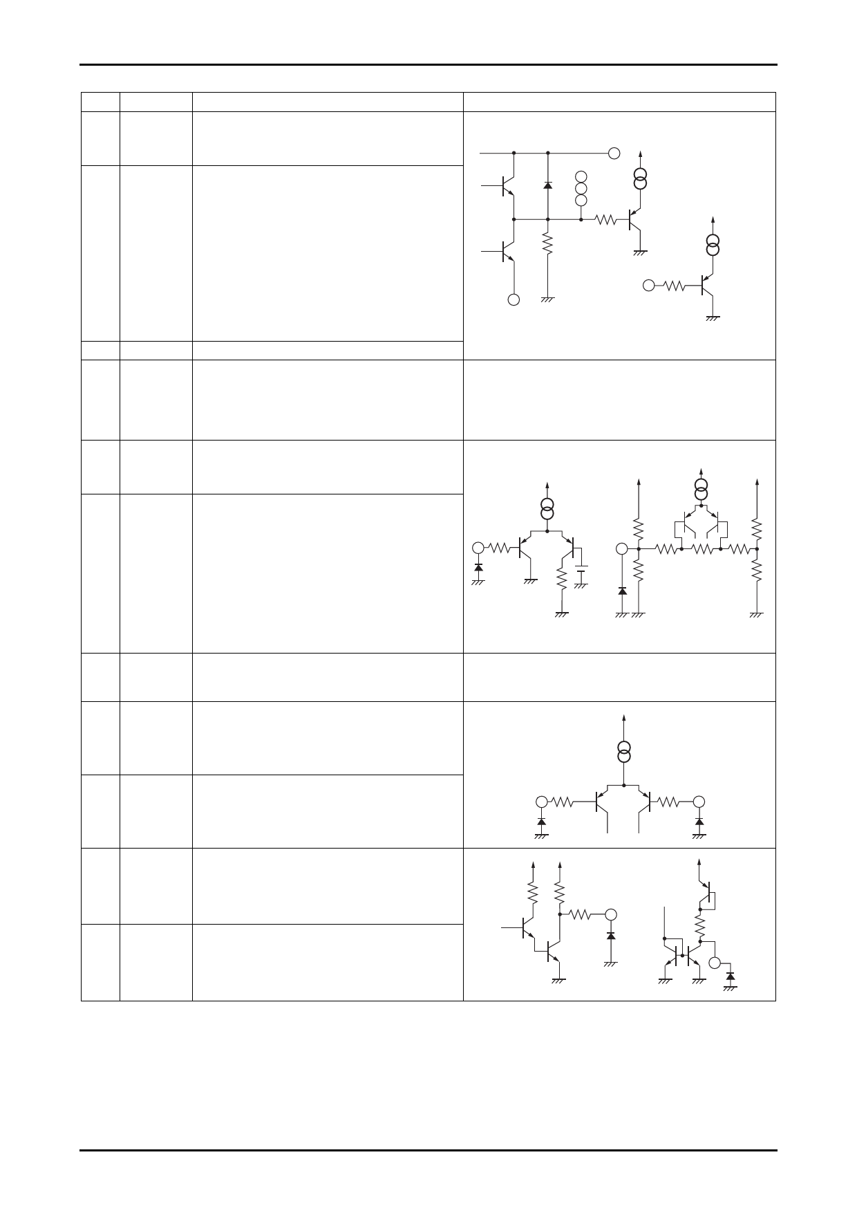
Pin Function
Pin No.
27
28
1
Pin Name
UOUT
VOUT
WOUT
Function
U phase output, Spark killer diodes are built-in.
V phase output, Spark killer diodes are built-in.
W phase output, Spark killer diodes are built-in.
4
Rf
Output current detection. The control block current limiter
(SENSE) operates using the resistor Rf connected between these
5
Rf
pins and ground. Also, the lower side saturation
(PWR)
prevention circuit and the torque ripple correction circuit
operate based on the voltages across this resistor. It is
especially important to note that, since the saturation
prevention level is set using this voltage, the lower side
saturation prevention circuit will become less effective in
the high current region if the value of Rf is lowered
excessively. Also, the PWR and SENSE pins must be
connected together.
22
VS
Output block power supply
5
GSENSE Ground sensing. The influence of the common ground
impedance on Rf can be excluded by connecting this pin
to nearest ground for the Rf resistor side of the motor
ground wiring that includes Rf. (This pin must not be left
open.)
6
FR
Forward / reverse selection. The voltage applied to this
pin selects the motor direction (forward or reverse).
(Vth=2.5V at VCC=5V (typical))
23
ADJ
Used for external adjustment of the torque ripple
correction ratio. Apply a voltage externally with a
low-impedance circuit to the ADJ pin to adjust the
correction ratio. The correction ratio falls as the applied
voltage is increased, and increases as the applied voltage
decreases. The torque ripple correction ratio can be
modified by factors in the range 0 to 2 times the ratio that
applies when his pin is left open. (The pin voltage is set to
about VCC / 2 internally, and the input impedance is about
5kΩ.)
7
GND
Ground for all circuits other than the output transistors.
The lowest potential of the output transistors is that of the
Rf pin.
8
FGIN-
Input used when the FG amplifier is used as an inverting
input. A feedback resistor must be connected between
FGOUT and this pin.
Equivalent circuit
22
VS
27
28
1 OUT
200Ω
30kΩ
VCC
150µA
Lower side saturation
prevention circuit input block
VCC
10µA
24
Rf (PWR)
200Ω
4
Rf (SENSE)
VCC
VCC
VCC
VCC
20µA
FR
6
200Ω
200µA
ADJ
23
1/2
VCC
10kΩ
6kΩ
10kΩ
10kΩ
500Ω
6kΩ
10kΩ
VCC
5µA
9
FGIN+
Non-inverting input used when the FG amplifier is used as
a differential input amplifier. No bias is applied internally.
FGIN(−)
9
300Ω
FGIN(+)
8
300Ω
10
FGOUT
FG amplifier output. There is an internal resistive load.
14
FC
Speed control loop frequency characteristics correction.
VCC
VCC
2kΩ
FGOUT
10
300Ω
VCC
10kΩ
14
FC
Continued on next page.
No.A0231-5/7
Share Link: 