LB8902 データシートの表示(PDF) - SANYO -> Panasonic
部品番号
コンポーネント説明
メーカー
LB8902 Datasheet PDF : 4 Pages
| |||
LB8902M
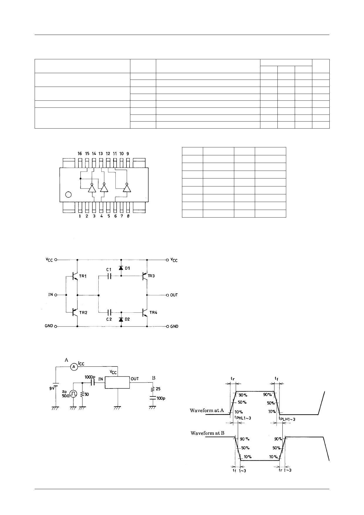
Switching Characteristics at Ta = 25˚C, VCC1=VCC2=9V, Vin=5Vp-p (f=14.3MHz), tr, tf≤6ns, load conditions :
RL=25Ω, CL=100pF
Parameter
Symbol
Conditions
Ratings
Unit
min
typ
max
Propagation time
Transient time
Output amplitude
Current drain
tPLH1-3
tPHL1-3
tr1-3
tf1-3
VOP-P
ICC1
ICC2
ICC3
See Fig.A.
See Fig.A.
See Fig.A.
See Fig.A.
See Fig.A.
See Fig.A.
See Fig.A.
See Fig.A.
VCC–0.8
10
15 ns
8
15 ns
8
15 ns
8
15 ns
VCC Vp-p
32
mA
32
mA
32
mA
Pin Assignment
Pin No. Function Pin No.
1
Frame GND
9
2
GND
10
3
IN1
11
4
IN2
12
5
GND
13
6
IN3
14
7
N.C.
15
8
Frame GND
16
Note) Do not use the N.C. pin.
Function
Frame GND
N.C.
OUT3
VCC2
OUT2
OUT1
VCC1
Frame GND
Equivalent Circuit Block Diagram
Test Circuit
Unit (resistance : Ω, capacitance : F)
Fig. A Propagation Time, Transient Time
No.3029–2/4
Share Link: 