LC7219M データシートの表示(PDF) - SANYO -> Panasonic
部品番号
コンポーネント説明
メーカー
LC7219M Datasheet PDF : 12 Pages
| |||
LC7219, 7219M
Table 1. Input data bits
Bits
Name
1 to 16
D0 to D15
17 to 23
O0 to O6
24
CTEN
25 to 28
29, 30
31, 32
33
34
35, 36
R0 to R3
DV, SP
SC, SF
GT
TB
T0, T1
Description
Programmable divider ratio
D15 is the msb. The lsb is determined by the setting of the DV and SP flags as shown in table 6.
D0 to D3 are ignored if D4 is the lsb.
Output port data
Data bits O0 to O6 are latched into the OUT0 to OUT6 ports, respectively. When a data bit is 1,
the corresponding output pin is LOW, and when 0, HIGH. These outputs can be used for
frequency band selection.
If TB is 1, the O0 bit is ignored and the 8 Hz timebase signal is output on OUT0.
General-purpose counter enable
When CTEN is 0, the 20-bit general-purpose counter is reset and the HCTR and LCTR inuts are
pulled to ground. When the CTEN flag is 1, the counter is enabled and the signal on HCTR or
LCTR, selected by SC, is measured. Note that the general-purpose counter output should be
transferred to the external controller before CTEN is set to 0.
Reference frequency select
Bits R0 to R3 disable the PLL or select the reference frequency as shown in table 2. When the
PLL is disabled, the programmable divider is stopped, AMIN and FMIN are pulled to ground, and
the charge-pump outputs become high impedance.
Divider select and sensitivity select
DV select the local-oscillator input FMIN or AMIN. SP selects the input frequency range when
AMIN is selected as shown in table 6.
General-purpose counter input select and frequency/period measurement select
SC selects the general-purpose counter input. SF selects frequency or period measurement when
LCTR is selected as shown in table 7. When HCTR is selected, the counter is in frequency
measurement mode.
General-purpose counter time interval select
Bit GT selects the measurement time interval or the number of periods to be measured. When
GT=1, then 30 ms or 2 periods are selected, and when GT=0, 60 ms or 1 period is selected.
Timebase output enable
When TB is 1, the 8 Hz, 40% duty cycle timebase signal is output on OUT0. The O0 bits is
ignored.
Test control bits
Bits T0 to T1 are used for device testing and are set to 0 for normal operation.
Related bits
DV, SP
TB
SC, SF, GT
CTEN, GT
CTEN, SC, SF
O0
The reference frequency is selected by bits R0 to R3 as shown in table 2.
Table 2. Reference frequency selection
Table 2. Reference frequency selection–continued
R0
R1
R2
R3
0
0
0
0
0
0
0
1
0
0
1
0
0
0
1
1
0
1
0
0
0
1
0
1
0
1
1
0
0
1
1
1
Reference frequency (kHz)
100
50
25
25
12.5
6.25
3.125
3.125
R0
R1
R2
R3
1
0
0
0
1
0
0
1
1
0
1
0
1
0
1
1
1
1
0
0
1
1
0
1
1
1
1
0
1
1
1
1
Reference frequency (kHz)
10
9
5
1
PLL inhibit
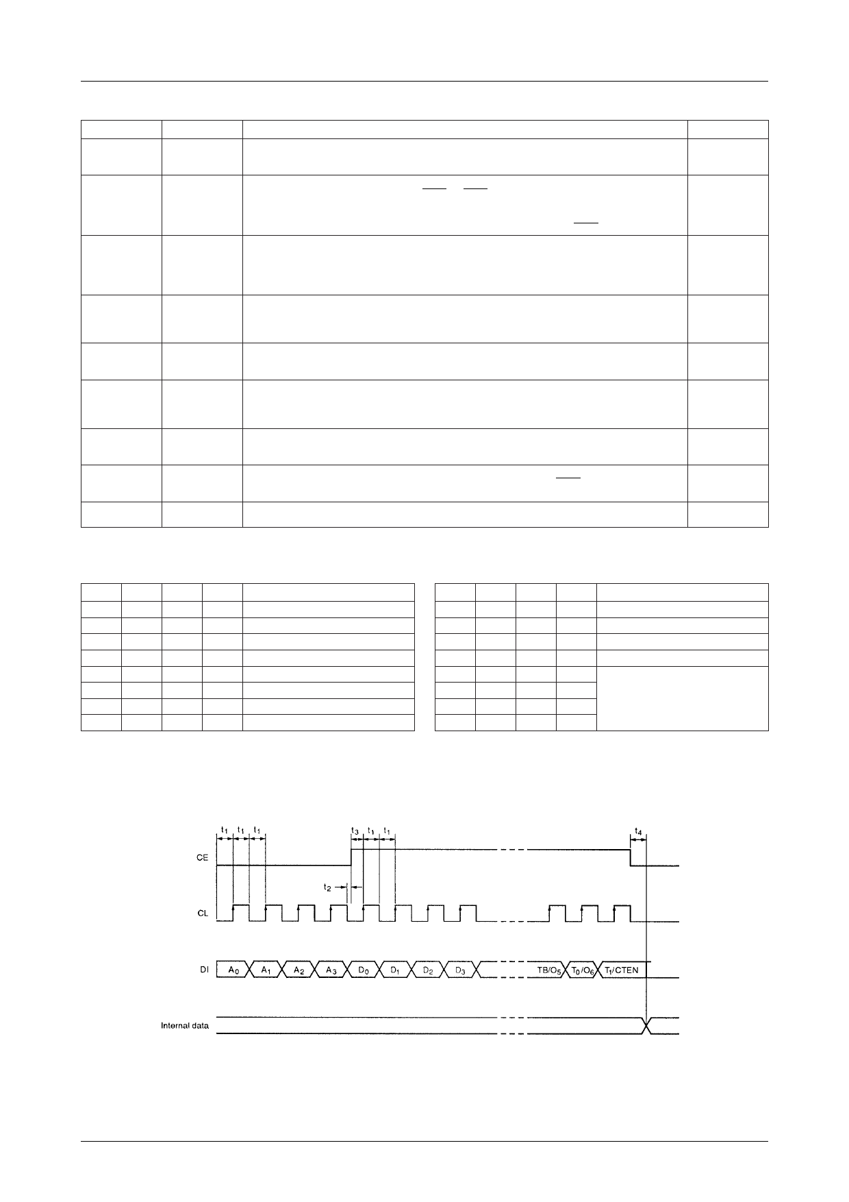
Serial Data Input Timing
The timing for the serial data input is shown in figure 2. The first four bits, A0 to A3, are the mode select bits.
In 36-bit transfer mode, the final data bits are T0 and T1, and in 24-bit transfer mode, O6 and CTEN.
Note
t1≥1.5µs, t2≥0µs, t3≥1.5µs, t4<1.5µs
Figure 2. Input timing
No.3661–5/12
Share Link: 