LC7219M データシートの表示(PDF) - SANYO -> Panasonic
部品番号
コンポーネント説明
メーカー
LC7219M Datasheet PDF : 12 Pages
| |||
LC7219, 7219M
Serial Data Output
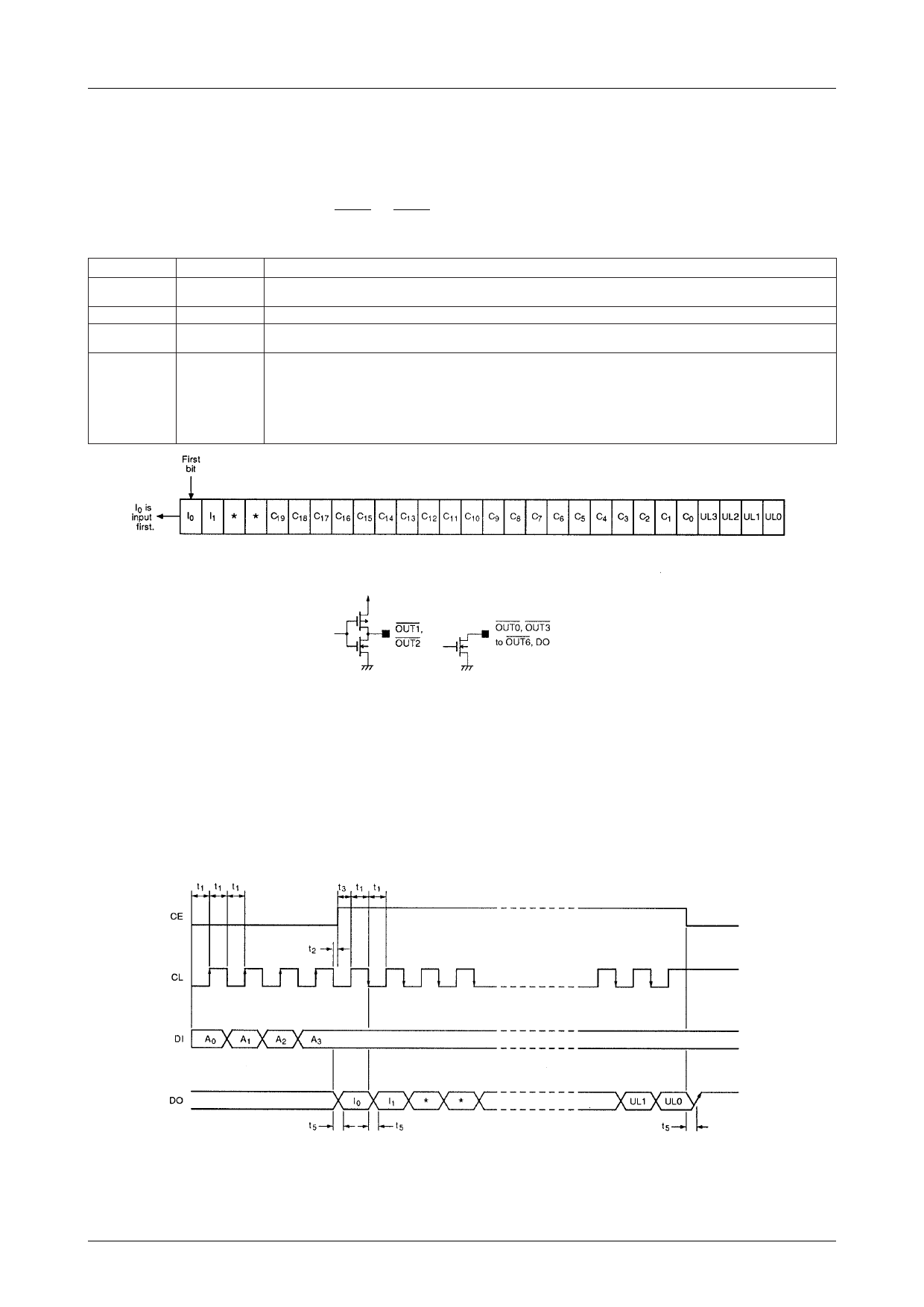
The LC7219 and LC7219M both have an internal 28-bit shift register that comprise two bits representing the state of
IN0 and IN1 (I0 and I1, respectively), a 20-bit general-purpose counter address (C0 to C19) and unlock flags (UL0 to
UL3) as shown in table 3.
The shift register contents are clocked out on DO when the serial data output mode is selected as shown in figure 3.
The internal circuit of outputs DO and OUT0 to OUT6 are shown in figure 4.
Table 3. Shift register data
Bits
Name
1, 2
I0, I1
3, 4
5 to 24
C0 to C19
25 to 28
UL3 to UL0
Description
Input port data
I0 is the state of IN0, and I1, the state of IN1.
Invalid
General-purpose counter value
Bits C0 to C19 are the latched value of the 20-bit counter. C19 is the msb.
PLL unlock status bits
Bits UL0 to UL3 are the latched data from the unlock detector circuit. When the phase error exceeds the value for a
given bit as shown below for a 7.2MHz crystal, the bit is set.
UL0 is set when ΦERROR ≥ 1.1µs
UL1 is set when ΦERROR ≥ 2.2µs
UL2 is set when ΦERROR ≥ 3.3µs
UL3 is set when ΦERROR ≥ 0.55µs
Figure 3. Shift register data format
Figure 4. Output driver internal circuits
Serial Data Output Timing
The timing for the serial data output is shown in figure 5. Bits A0 to A3 are the mode select bits. When CE goes HIGH,
I0 is output on DO, and each subsequent data bit is output on the falling edge of CL. CE should be held HIGH for 27
clock cycles to allow all data to be output.
In serial data output mode, DO is forced HIGH when CE goes LOW as shown in figure 5. DO goes LOW when the
status of IN0 changes. In frequency or period measurement modes, DO goes LOW when frequency or period measure-
ment is completed.
Note
t1≥1.5µs, t2≥0µs, t3≥1.5µs, t5<1.5µs
Figure 5. Output timing
No.3661–6/12
Share Link: 