LC723461W データシートの表示(PDF) - SANYO -> Panasonic
部品番号
コンポーネント説明
メーカー
LC723461W Datasheet PDF : 13 Pages
| |||
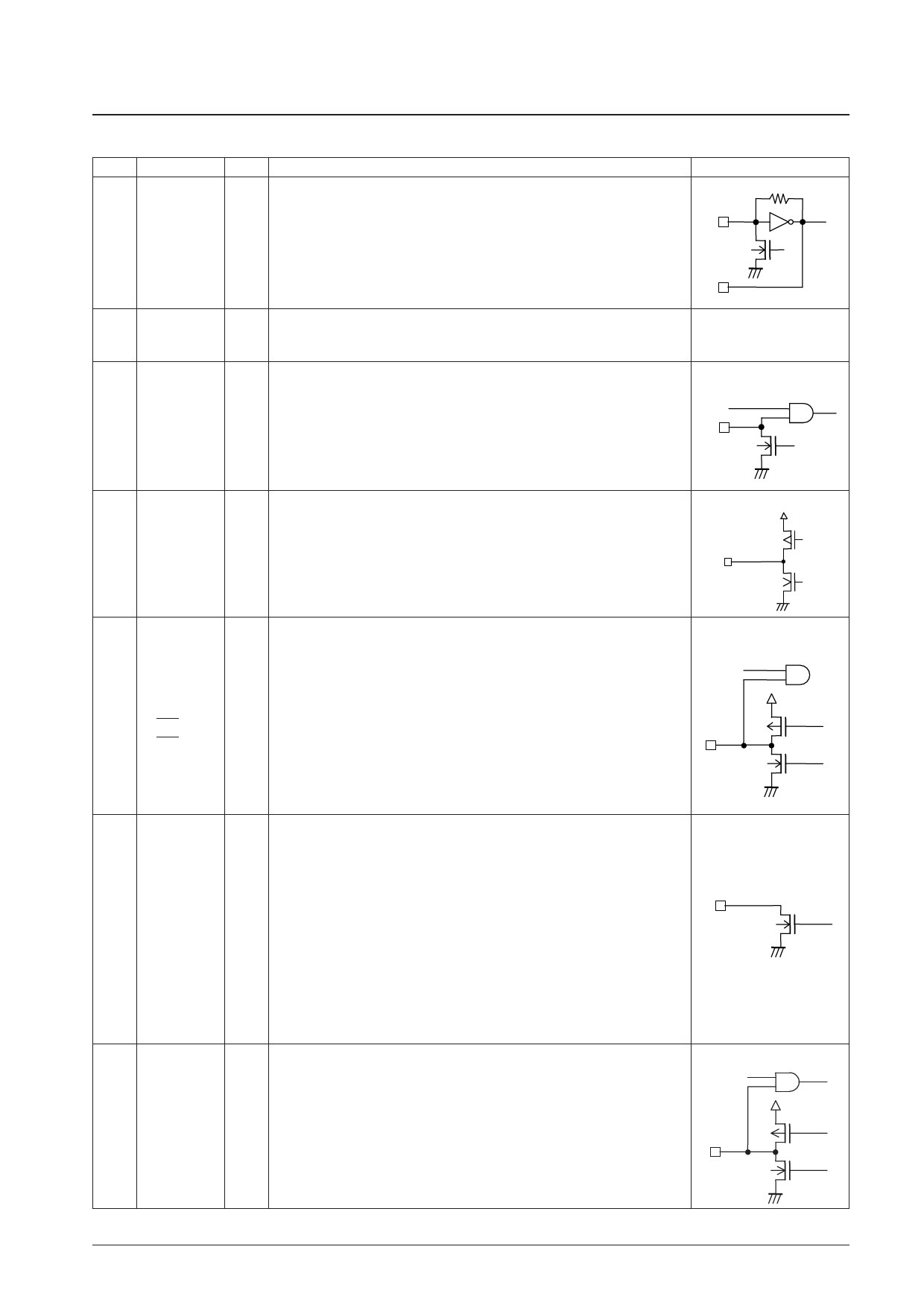
Pin Functions
Pin No.
Pin
I/O
LC723461W, 723462W
Function
64
XIN
I
75 kHz oscillator connections
1
XOUT
O
I/O circuit
63
TEST1
5
PA0
4
PA1
3
PA2
2
PA3
I
IC testing.
This pin must be connected to ground.
Special-purpose ports for key return signal input designed with a low threshold
voltage. When a key matrix is formed in combination with port PB, simultaneous
I
multiple key presses with up to 3 keys can be detected. The pull-down resistors are
set up for all four pins at the same time with the IOS instruction. This setting cannot
be specified for individual pins. In backup mode, these pins go to the input disabled
state, and the pull-down resistors are disabled after a reset.
—
Input with built-in
pull-down resistor
Unbalanced CMOS push-pull
9
PB0
Unbalanced CMOS outputs. Since these outputs are unbalanced, no diodes are
8
PB1
required to prevent short circuits due to simultaneous multiple key presses. These
O outputs go to the high-impedance output state in backup mode. After a reset, they go
7
PB2
to the high-impedance output state and remain in that state until an output instruction
6
PB3
(OUT, SPB, or RPB) is executed.
13
PC0
12
PC1
General-purpose I/O ports. Note that there is a mask option that allows these pins to
11
PC2
be used as n-channel open drain ports.
18
PC3
I/O
PD0, PD1 can be used as an external interrupt port. The IOS instruction (Pwn = 4, 5)
is used for switching the general-purpose I/O port function, and these ports can be set
17
INT1/PD0
to input or output in 1-bit units. (0: input, 1: output)
16
INT0/PD1
In backup mode they go to the input disabled high-impedance state.
15
PD2
After a reset, they switch to the general-purpose input port function.
14
PD3
CMOS push-pull/
N-ch open-drain
General-purpose output ports. Note that PE0 has a shared function as the BEEP
output, and that PE1 has a shared function as a D/A converter output port. Since
these ports are open drain ports, a resistor must be inserted between each port and
VDD. At reset, they are set to the general-purpose output port function .The BEEP
instruction is used to switch the BEEP/PE0 port between the general-purpose output
port and the BEEP output functions. A BEEP instruction with b2 = 0 will set the
BEEP/PE0 port to function as a general-purpose output port. If b2 is set to 1, the
19
BEEP/PE0
O instruction will select the BEEP output function. Bits b0 and b1 switch the frequency of
the BEEP output. This IC supports two BEEP frequencies.
18
DAC/PE1
*: When the PE0 port is set to function as the BEEP output, executing an output
instruction for PE0 will only change the value of the internal output latch; it will have
no effect on the output.
The DAC instruction is used to switch the DAC/PE1 port between the general-purpose
output port and DAC output functions. These ports go to the high-impedance state in
backup mode. That state is maintained until an output instruction, a BEEP instruction,
or a DAC instruction is executed.
Shared function pins used as either general-purpose I/O ports or a serial I/O port.
Note that there is a mask option that allows these pins to be used as n-channel open
25
SCK1/PK1
drain ports. When used as general-purpose I/O ports, the I/O direction can be
switched in single pin units with the IOS instruction. The IOS instruction is used to
24
SO1/PK2
I/O switch the function between the general-purpose I/O port and the serial I/O port
23
SI1/PK3
function.
In backup mode, these pins go to the input disabled high-impedance state. After a
reset, the general-purpose input port function is selected.
N-ch open-drain
CMOS push-pull/
N-ch open-drain
Continued on next page.
No. 7275-7/13
Share Link: 