LC72725M(2003) データシートの表示(PDF) - SANYO -> Panasonic
部品番号
コンポーネント説明
メーカー
LC72725M Datasheet PDF : 8 Pages
| |||
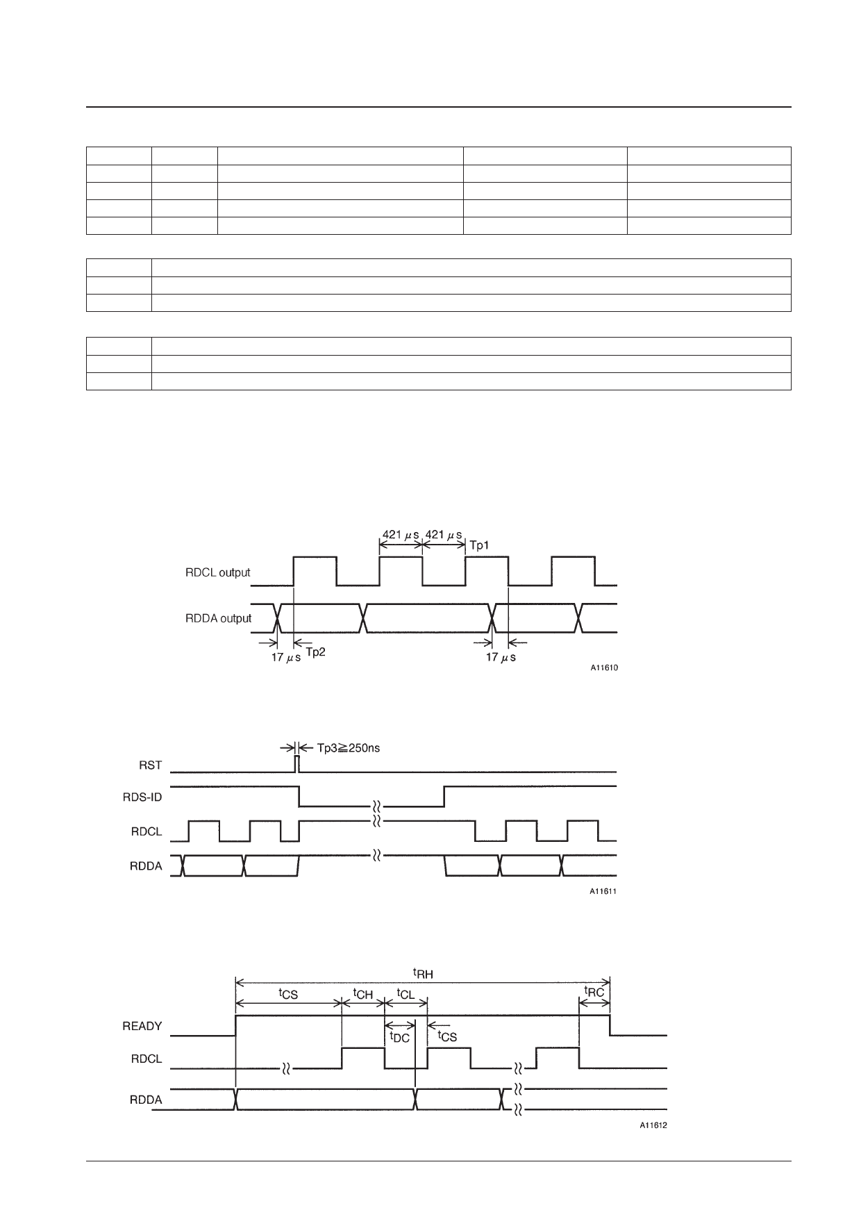
RDCL/RDDA Output Timing
• Master mode
LC72725M, LC72725V
RST Operation
• Master mode
RDCL Control in Slave Mode
Caution: After an RST input, the
RDCL and RDDA outputs
stop at the high level until
the first RDS ID detection.
Parameter
RDCL setup time
RDCL high-level time
RDCL low-level time
Data output time
READY output time
Ready high-level time
Symbol
Conditions
tCS RDCL, RDDA
tCH RDCL
tCL
RDCL
tDC RDCL, RDDA
tRC RDCL, READY
tRH READY
min
0
0.75
0.75
Ratings
typ
Unit
max
µs
µs
µs
0.75
µs
0.75
µs
107 ms
Notes:1. Start RDCL clock input after the READY signal goes high. Applications must stand by with RDCL held low when the READY pin is low.
2. Each time the RDCL input is switched from low to high to low, the application must check the READY signal level after the period tRC has elapsed
once RDCL has been set low. If READY is at the high level, the application may apply the next RDCL clock cycle. If READY is low, the application
must stop RDCL input at that point.
3. When the above timing conditions are met, RDDA can be read at either the rise or fall of the RDCL signal.
4. After the last data from memory has been read, READY will be low once the period tRC has elapsed after the fall of the RDCL signal. If even 1 bit of
data has been written to memory, READY will be high and the application will be able to read that data.
No. 7672-6/8
Share Link: 