LC74731 データシートの表示(PDF) - SANYO -> Panasonic
部品番号
コンポーネント説明
メーカー
LC74731 Datasheet PDF : 38 Pages
| |||
LC74731W,74732W
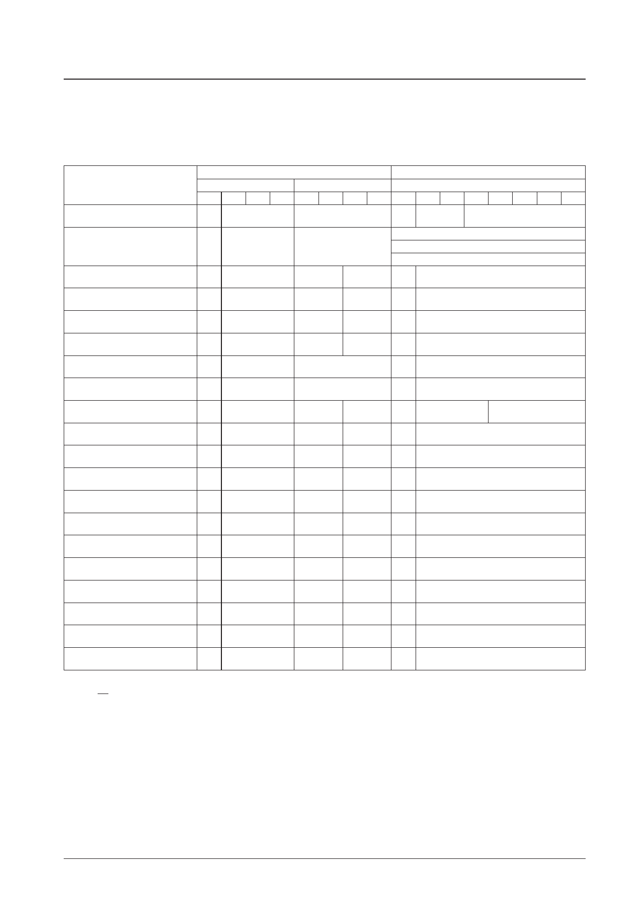
Display Control Commands
Display control commands have an 8-bit format and are transferred using the serial input function. Commands consist of
a command identification code in the first byte and command data in the following bytes.
Display Control Commands
Command
COMMAND0
(Write address setup)
COMMAND1 (Character write)
COMMAND20
(Vertical display start position)
COMMAND21
(Horizontal display start position)
COMMAND22
(Character size)
COMMAND23
(Character size - in line units)
COMMAND3
(Display control)
COMMAND4
(Display control)
COMMAND50
(Sync signal detection 1)
COMMAND51
(Sync signal detection 2)
COMMAND52
(Display control)
COMMAND53
(Display control)
COMMAND60
(Outlining setting)
COOMAND61
(Outlining setting - in line units)
COMMAND62
(Line spacing)
COMMAND63
(Line spacing - in line units)
COMMAND70
(Display level)
COMMAND71
(Display level - in line units)
COMMAND72
(Halftone - in line units)
COMMAND73
(RGB control)
First byte
Second byte
Command identification code
Data
Data
7
6
5
4
3
2
1
0
7
6
5
4
3
2
1
0
1
0
0
0 V3 V2 V1 V0 0
0
0 H4 H3 H2 H1 H0
at2 at1 CB2 CB1 CB0 CC2 CC1 CC0
1
0
0
1 IR SD2 SD1 SD0 0
0
0 C12 C11 C10 C9 C8
C7 C6 C5 C4 C3 C2 C1 C0
1
0
1
0
0
0 RRM1 RRM0 0 VP6 VP5 VP4 VP3 VP2 VP1 VP0
1
0
1
0
0
1
0
0
0 HP6 HP5 HP4 HP3 HP2 HP1 HP0
1
0
1
0
1
0
0 SRM 0
0
0
0 VS1 VS0 HS1 HS0
1
0
1
0
1
1
0 LSZUD 0
0 LSZB5 LSZA4 LSZ93 LSZ82 LSZ71 LSZ60
1
0
1
1 TSTMOD RAMERS OSCSTP SYSRST 0 LCSOFF XN53S BLKSEL LC FS BK DSPON
1
1
0
0 NP2 NP1 NP0 I/N 0 HLFINT BCL1 BCL0 CB PH2 PH1 PH0
1
1
0
1
0
0 DISLIN I/E 0 RN2 RN1 RN0 SN3 SN2 SN1 SN0
1
1
0
1
0
1 MUT1 MUT0 0
O RNE0 SJN3 SJN2 SJN1 SJC1 SJC0
1
1
0
1
1
0 EVEBSS LSPSS 0 CINSEL CINCTL VNPSEL VSPSEL MSKERS MSKSEL EGLSEL
1
1
0
1
1
1 RSLG1 RSLG0 0
0 CTL3 SPOSEL PALAL4 IHSEL VSSEL HSSEL
1
1
1
0
0
0
0 BRM 0 BXBLV1 BXBLV0 BXWLV1 BXWLV0 ATSEL BLK1 BLK0
1
1
1
0
0
1
0 LFCUD 0
0 LFCB5 LFCA4 LFC93 LFC82 LFC71 LFC60
1
1
1
0
1
0
0 GRM 0
O BXC1 GS1 GS0 GY2 GY1 GY0
1
1
1
0
1
1
0 LGYUD 0
0 LGYB5 LGYA4 LGY93 LGY82 LGY71 LGY60
1
1
1
1
0
0
0 LRM 0
0 BKLC1 BKLC0 CHLC1 CHLC0 RSLC1 RSLC0
1
1
1
1
0
1
0 LCLUD 0
0 LCLB5 LCLA4 LCL93 LCL82 LCL71 LCL60
1
1
1
1
1
0 LHTDAT LHTUD 0
0 LHTB5 LHTA4 LHT93 LHT82 LHT71 LHT60
1
1
1
1
1
1
0
0
0 DASSS GBSEL OUTSEL HSPSW XONSS BLK01 BLK00
Note that when the display character data write command (COMMAND1) is written, tthese ICs lock into the display character data write mode, and another
first byte cannot be written.
When the CS pin is set high, the these ICs are set to the COMMAND0 (display memory write address setup mode) state.
No. 6526-10/38
Share Link: 