LC78631 データシートの表示(PDF) - SANYO -> Panasonic
部品番号
コンポーネント説明
メーカー
LC78631 Datasheet PDF : 34 Pages
| |||
LC78631E
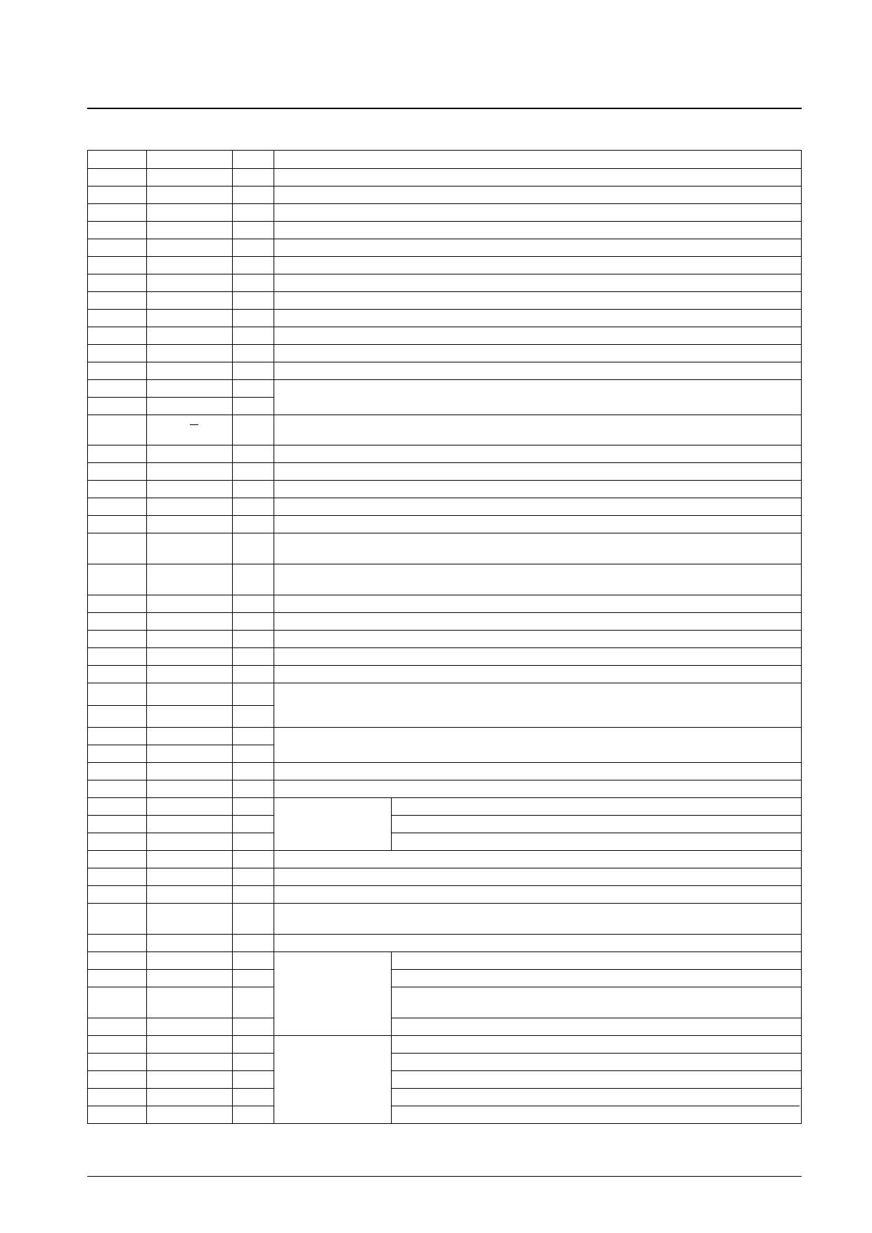
Pin Functions
Pin No.
1
2
3
4
5
6
7
8
9
10
11
12
13
14
15
16
17
18
19
20
21
22
23
24
25
26
27
28
29
30
31
32
33
34
35
36
37
38
39
40
41
Symbol
VPDO
PDO2
PDO1
AVSS
FR
AVDD
ISET
TAI
EFMO
VSS
EFMI
TEST1
CLV+
CLV–
V/P
TEST2
TEST3
P4
HFL
TES
PCK
FSEQ
TOFF
TGL
THLD
TEST4
VDD
JP+
JP–
SLD+
SLD–
EMPH
P5
LRCKO
DFLRO
DACKO
CONT1
P0/DFCK
P1/DFIN
P2
P3/DFLR
I/O
Function
O Variable pitch PLL charge pump output. Must be left open if unused.
O Double-speed and quad-speed mode playback PLL charge pump output. Must be left open if unused.
O Normal-speed mode playback PLL charge pump output
Analog system ground. Must be connected to 0 V.
Built-in VCO frequency range setting resistor connection
Analog system power supply
PDO1 and PDO2 output current setting resistor connection
I
Test input. A pull-down resistor is built in. Must be connected to 0 V.
O EFM signal output
Digital system ground. Must be connected to 0 V.
I
EFM signal input
I
Test input. A pull-down resistor is built in. Must be connected to 0 V.
O
Spindle servo control output. CLV+ outputs a high level for acceleration, and CLV– outputs a high level for
O deceleration.
Rough servo/phase control automatic switching monitor output. A high-level output indicates rough servo, and a
O
low-level output indicates phase control.
I
Test input. A pull-down resistor is built in. Must be connected to 0 V.
I
Test input. A pull-down resistor is built in. Must be connected to 0 V.
I/O I/O port
I
Track detection signal input. This is a Schmitt input.
I
Tracking error signal input. This is a Schmitt input.
O
EFM data playback bit clock monitor. Outputs 4.3218 MHz when the phase is locked in normal-speed mode
playback.
Synchronization signal detection output. Outputs a high level when the synchronization signal detected from the
O
EFM signal matches the internally generated synchronization signal.
O Tracking off output
O Tracking gain switching output. Increase the gain when this pin outputs a low level.
O Tracking hold output
I
Test input. A pull-down resistor is built in. Must be connected to 0 V.
Digital system power supply
O
Track jump output. JP+ outputs a high level both for acceleration during outward direction jumps and for
deceleration during inward direction jumps. JP– outputs a high level both for acceleration during inward direction
O jumps and for deceleration during outward direction jumps.
O
Sled output. This pin can be set to 1 of 4 levels by commands sent from the system control microprocessor.
O
O De-emphasis monitor. A high level indicates that a disk requiring de-emphasis is being played.
I/O I/O port
O
LR clock output
O
Digital filter outputs
LR data output. The digital filter can be turned off with the DFOFF command.
O
Bit clock output
O Output port
I/O I/O port. DF bit clock input in antishock mode.
I/O I/O port. DF data input in antishock mode.
I/O port. Used as the de-emphasis filter on/off switching pin in antishock mode. The de-emphasis filter is turned
I/O on when this pin is high.
I/O I/O port output or digital filter LR clock input (when anti-shock mode)
42
LRSY
O
43
CK2
O
ROMXA pins
44
ROMXA
O
45
C2F
O
46
MUTEL
O
47
LVDD
48
LCHP
O
One-bit D/A
49
LCHN
O
converter pins
50
LVSS
LR clock output
Bit clock output. The polarity can be inverted with the CK2CON command.
Interpolated data output. Data that has not been interpolated can be output by issuing
the ROMXA command.
C2 flag output
Left channel mute output
Left channel power supply
Left channel P output
Left channel N output
Left channel ground. Must be connected to 0V.
Note: Of the general-purpose I/O ports, any unused input ports must be connected to 0 V, or set to be output ports.
Continued on next page.
No. 5342-8/34
Share Link: 