LC9997 データシートの表示(PDF) - SANYO -> Panasonic
部品番号
コンポーネント説明
メーカー
LC9997 Datasheet PDF : 11 Pages
| |||
Point B
Point A
LC9997M
VB · TND
SM = —————
× 100 [%]
250
VB: The amount of smear at point B (mV)
TND: The transmittance of the neutral density
filters used.
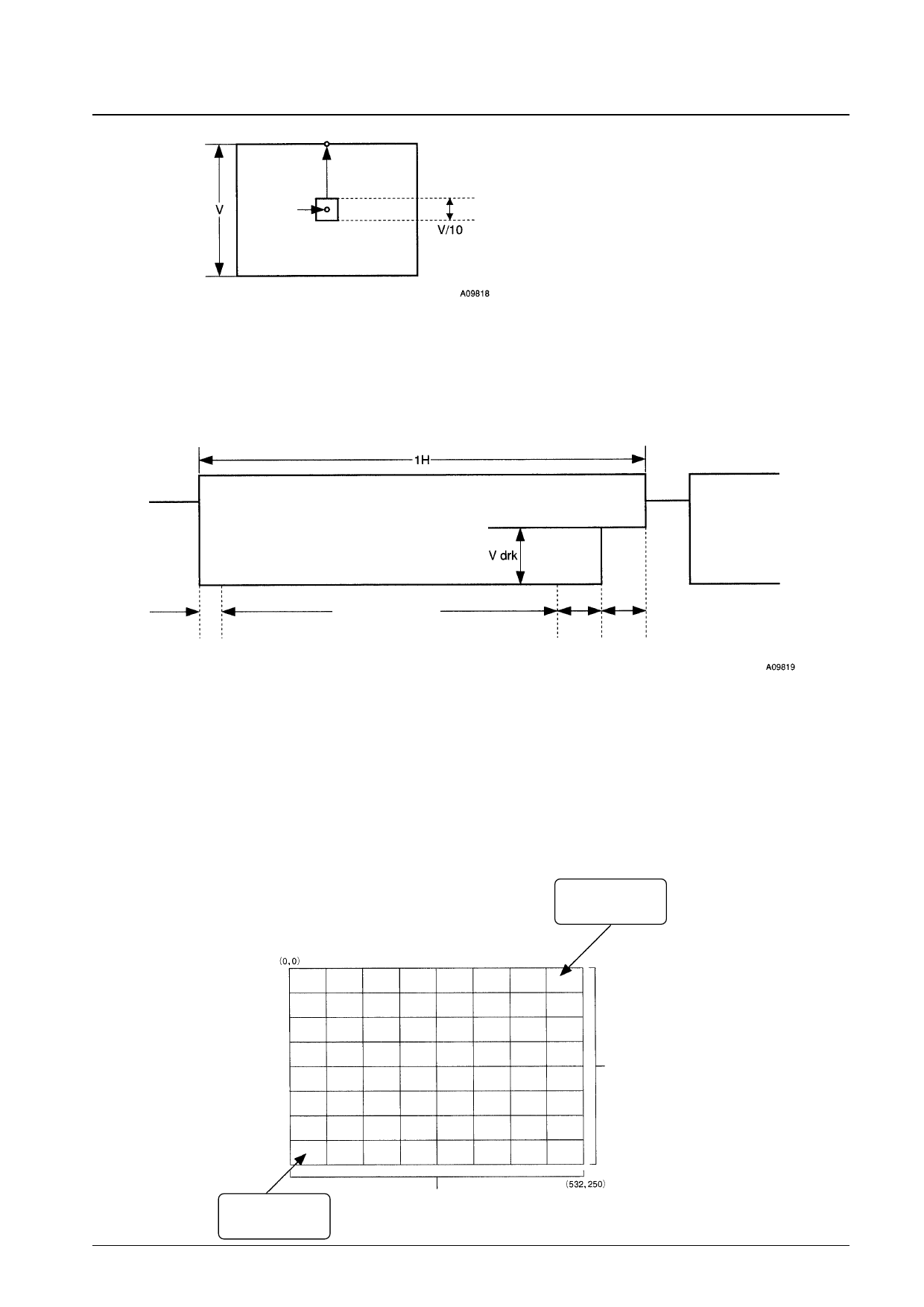
5. Dark signal
Block all light from the surface of the CCD element, and measure the CCD output signal at the center of the screen.
For this measurement, do not measure the difference between the signal level and the optical black area level, but
rather, read out the difference with the no-signal level at a point where there is no pixel information. (See the figure.)
Structure of the Horizontal Period
Effective pixel area
Optical black area
Optical black area No-signal area
6. Color irregularity (mura)
With no pattern in the LV-2001 pattern box, image the pattern box with a C-500 1-mm thick IR cut filter and a 7%
neutral density filter over the whole surface of the 1/5-inch standard lens used for measurement. Verify that the CCD
average output at this time is over 200 mV. Calculate the color difference signals RY and BY from the following
formula from the average output of post-image processing R, G, and B signals. The color irregularity (mura) CS is
defined as the distance between the two points for which the data (RY and BY) is separated the most for all the areas.
RY = {(red-green) – (blue-green) × 0.25} × 101/64
BY = {(blue-green) – (red-green) × 0.125} × 50/64
CS = {(RY1-RY2)2 + (BY1-BY2)2}1/2
Color Irregularity (mura) Data Acquisition Areas
In each block:
V direction: 30 pixels
H direction: 60 pixels
Divided into 8 areas of equal separation.
In each block:
V direction: 30 pixels
H direction: 60 pixels
Divided into 8 areas of equal separation.
No. 5783-8/11
Share Link: 