TC1263 データシートの表示(PDF) - Microchip Technology
部品番号
コンポーネント説明
メーカー
TC1263 Datasheet PDF : 14 Pages
| |||
TC1263
2.0 PIN DESCRIPTIONS
The descriptions of the pins are listed in Table 2-1.
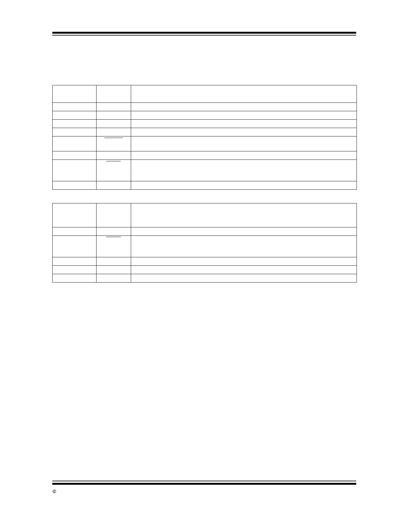
TABLE 2-1: PIN FUNCTION TABLE
Pin No.
(8-Pin SOIC)
1
2
3
4
5
6
7
8
Symbol
Description
VOUT
GND
NC
BYPASS
ERROR
NC
SHDN
VIN
Regulated voltage output.
Ground terminal.
No connect.
Reference bypass input. Connecting a 470pF to this input further reduces output noise.
Out-of-Regulation Flag (open drain output). This output goes low when VOUT is out-of-tolerance
by approximately – 5%.
No connect.
Shutdown control input. The regulator is fully enabled when a logic high is applied to this input.
The regulator enters shutdown when a logic low is applied to this input. During shutdown, output
voltage falls to zero and supply current is reduced to 0.05µA (typical).
Unregulated supply input.
Pin No.
(5-Pin DDPAK)
(5-Pin TO-220)
1
2
3
4
5
Symbol
Description
BYP
SHDN
GND
VIN
VOUT
Reference bypass input. Connecting a 470pF to this input further reduces output noise.
Shutdown control input. The regulator is fully enabled when a logic high is applied to this input.
The regulator enters shutdown when a logic low is applied to this input. During shutdown, output
voltage falls to zero and supply current is reduced to 0.05µA (typical).
Ground terminal.
Unregulated supply input.
Regulated voltage output.
© 2002 Microchip Technology Inc.
DS21374B-page 3
Share Link: 