LT1120AC データシートの表示(PDF) - Linear Technology
部品番号
コンポーネント説明
メーカー
LT1120AC Datasheet PDF : 8 Pages
| |||
LT1120A
PI FU CTIO S
GND (Pin 1): Ground
FEEDBACK (Pin 2): This is the feedback point of the
regulator. When operating, it is nominally at 2.5V.
Optimum source resistance is 200k to 500k. The feedback
pin should not be driven below ground or more positive
than 5V.
SHUTDOWN (Pin 3): A logic 1 shuts off main regulator.
Caution: noise or leakage into the shutdown pin can affect
output voltage.
VOUT (Pin 4): Main output, requires 10µF output capaci-
tor. Can be shorted to VIN or ground without damaging
device.
VIN (Pin 5): Input Supply. Bypass with 10µF capacitor.
Must always be more positive than ground.
REF (Pin 6): Reference. 2.5V can source or sink current.
May be shorted to ground or up to 5V. Voltages in excess
of 5V can damage the device.
COMP OUT (Pin 7): Open Collector NPN Output. May be
connected to any voltage from ground to 36V more
positive than ground (operates above VIN). Short-circuit
protected.
–INPUT (Pin 8): Inverting Comparator Input.
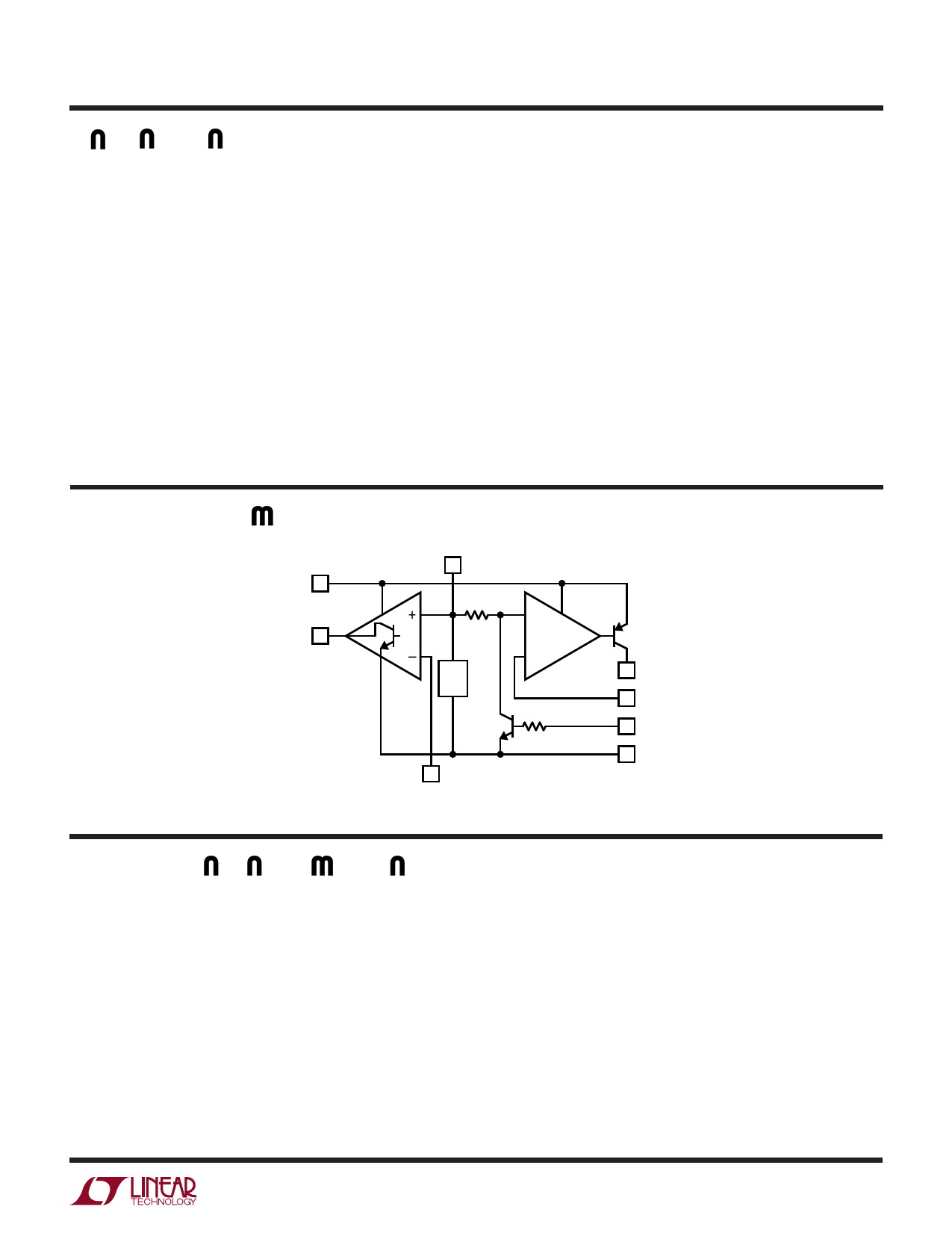
BLOCK DIAGRA
VIN 5
COMP OUT 7
REF
6
100k
REF
2.5V
120k
8
–INPUT
4 VOUT
2 FEEDBACK
3 SHUTDOWN
1 GROUND
1120A BD01
APPLICATIO S I FOR ATIO
The LT1120A is especially suited for micropower system
applications. For example, the comparator section of the
LT1120A may be used as a battery checker to provide an
indication of low battery. Another type of system applica-
tion for the LT1120A would be to generate the equivalent
of split supplies off of a single power input. The regulator
section provides regulated output voltage and the
reference, which can both source and sink current is then
an artificial system ground providing a split supply for
the system.
For many applications the comparator can be frequency
compensated to operate as an amplifier. Compensation
values for various gains are given in the data sheet. The
comparator gain is purposely low to make it easier to
frequency compensate as an amplifier. The NPN output is
capable of sinking 10mA and can drive loads connected to
voltages in excess of the positive power supply. This is
useful for driving switches or linear regulators off of a
higher input voltage.
1120afa
5
Share Link: 