LT1242 データシートの表示(PDF) - Linear Technology
部品番号
コンポーネント説明
メーカー
LT1242 Datasheet PDF : 16 Pages
| |||
LT1241 Series
PI FU CTI S
COMP (Pin 1): Compensation Pin. This pin is the output of
the Error Amplifier and is made available for loop compen-
sation. It can also be used to adjust the maximum value of
the current sense clamp voltage to less than 1V. This pin
can source a minimum of 0.5mA (0.8mA typ) and sink a
minimum of 2mA (4mA typ)
FB (Pin 2) Voltage Feedback Pin. This pin is the inverting
input of the error amplifier. The output voltage is normally
fed back to this pin through a resistive divider. The non-
inverting input of the error amplifier is internally commit-
ted to a 2.5V reference point.
ISENSE (Pin 3): Current Sense Pin. This is the input to the
current sense comparator. The trip point of the compara-
tor is set by, and is proportional to, the output voltage of
the Error Amplifier.
RT/CT (Pin 4): The oscillator frequency and the deadtime
are set by connecting a resistor (RT) from VREF to RT/CT
and a capacitor (CT) from RT/CT to GND.
The rise time of the oscillator waveform is set by the RC
time constant of RT and CT. The fall time, which is equal to
the output deadtime, is set by a combination of the RC time
constant and the oscillator sink current (8.2mA typ).
GND (Pin 5): Ground.
OUTPUT (Pin 6): This pin is the output of a high current
totem pole output stage. It is capable of driving up to ±1A
of current into a capacitive load such as the gate of a
MOSFET.
VCC (Pin 7): This pin is the positive supply of the control
IC.
VREF (Pin 8): Reference. This is the reference output of the
IC. The reference output is used to supply charging current
to the external timing resistor RT. The reference provides
biasing to a large portion of the internal circuitry, and is
used to generate several internal reference levels includ-
ing the VFB level and the current sense clamp voltage.
APPLICATI S I FOR ATIO
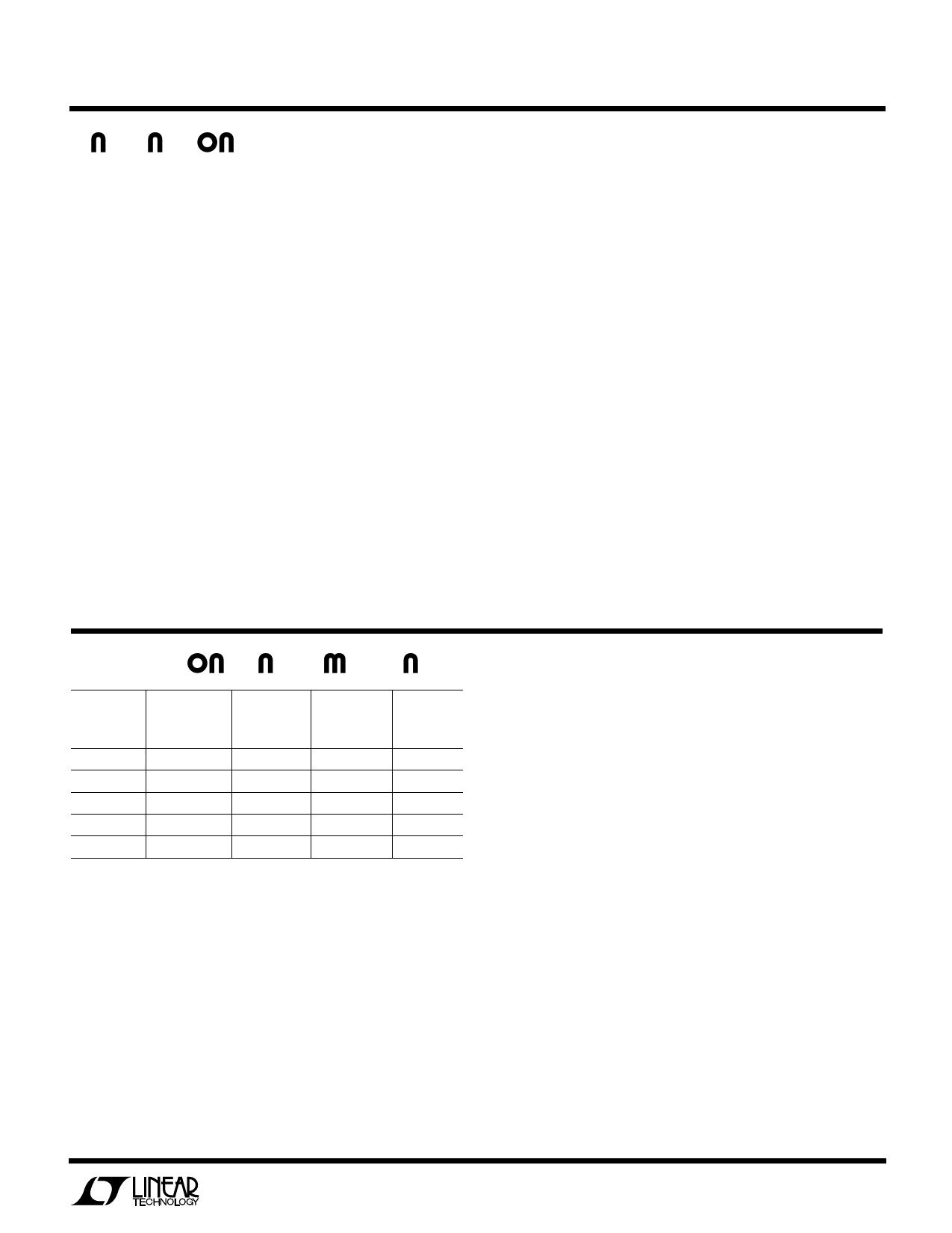
START-UP
DEVICE
LT1241
LT1242
LT1243
LT1244
LT1245
MINIMUM
OPERATING
THRESHOLD
9.6V
16V
8.4V
16V
8.4V
MAXIMUM
VOLTAGE
7.6V
10V
7.6V
10V
7.6V
DUTY CYCLE REPLACES
50%
NONE
100%
UC1842
100%
UC1843
50%
UC1844
50%
UC1845
Oscillator
The LT1241 series devices are fixed frequency current
mode pulse width modulators. The oscillator frequency
and the oscillator discharge current are both trimmed and
tightly specified to minimize the variations in frequency
and deadtime. The oscillator frequency is set by choosing
a resistor and capacitor combination, RT and CT. This RC
combination will determine both the frequency and the
maximum duty cycle. The resistor RT is connected from
VREF (Pin 8) to the RT/CT pin (Pin 4). The capacitor CT is
connected from the RT/CT pin to ground. The charging
current for CT is determined by the value of RT. The
discharge current for CT is set by the difference between
the current supplied by RT and the discharge current of the
LT124X. The discharge current of the device is trimmed to
8.2mA. For large values of RT discharge time will be
determined by the discharge current of the device and the
value of CT. As the value of RT is reduced it will have more
effect on the discharge time of CT. During an oscillator
cycle capacitor CT is charged to approximately 2.8V and
discharged to approximately 1.1V. The output is enabled
during the charge time of CT and disabled, in an off state,
during the discharge time of CT. The deadtime of the circuit
is equal to the discharge time of CT. The maximum duty
cycle is limited by controlling the deadtime of the oscilla-
tor. There are many combinations of RT and CT that will
yield a given oscillator frequency, however there is only
one combination that will yield a specific deadtime at that
frequency. Curves of oscillator frequency and deadtime
7
Share Link: 