LT1248 データシートの表示(PDF) - Linear Technology
部品番号
コンポーネント説明
メーカー
LT1248 Datasheet PDF : 12 Pages
| |||
LT1248
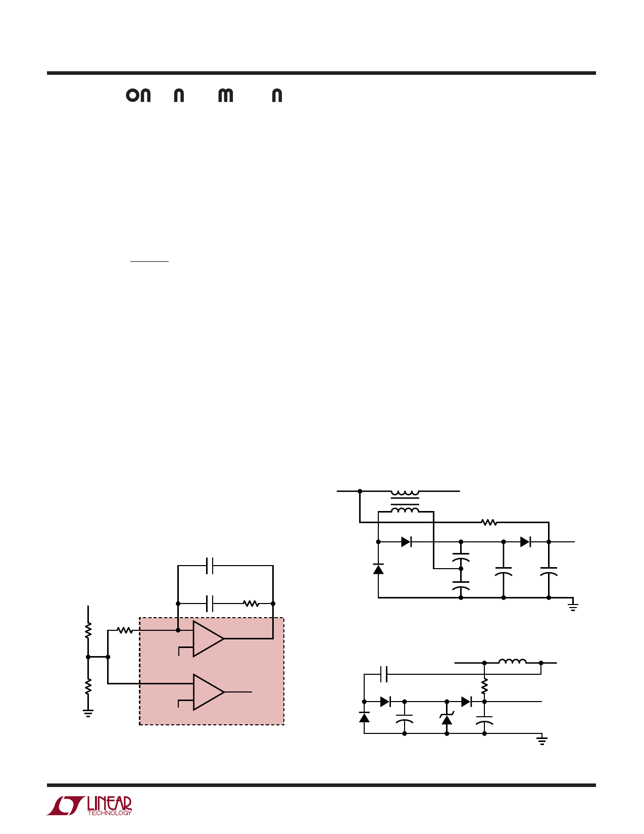
APPLICATI S I FOR ATIO
Note that VSENSE is the summing node and it stays at 7.5V.
When overshoot occurs on VOUT, the overcurrent from R1
will go through R2 as well as R3. Amplifier feedback will
keep VSENSE locked at 7.5V. The equivalent AC resistance,
seen by the comparator input pin OVP, is R2 in parallel
with R3, which is 10k. Therefore, with the comparator trip
level of 1.05VREF and R3 of 20k, the comparator trips when
VOUT overshoot exceeds 10%. Overvoltage trip level:
%VOUT
=
5%
R2 + R3
R3
MOUT is a high impedance current output. In the current
loop, offset line current is determined by multiplier offset
current and input offset voltage of the current amplifier.
A – 4mV current amplifier VOS translates into 20mA line
current and 5W input power for 250V line if 0.2Ω sense
resistor is used. Under no load or when the load power is
less than this offset input power, VOUT would slowly
charge up to an overvoltage state because the overvoltage
comparator can only reduce multiplier output current to
zero. This does not guarantee zero output current if the
current amplifier has offset. To regulate VOUT under this
condition, the amplifier M1 (see Block Diagram), becomes
active in the current loop when VAOUT goes down to 2.2V.
The M1 can put out up to 7µA to the resistor at the ISENSE
pin to cancel any current amplifier negative VOS and keep
VOUT error to within 2V.
0.047µF
REGULATOR OUTPUT
VOUT = 382V
R3
20k
R1
1M
R2
20k
C1
0.47µF
330k
VSENSE
–
+
VREF = 7.5V
OVP
–
VAOUT
ERROR AMP
LT1248
+
1.05VREF
OVERVOLTAGE
COMPARATOR
1248 F04
Figure 4
Undervoltage Lockout
The LT1248 turns on when VCC is higher than 16V and
remains on until VCC falls below 10V, whereupon the chip
enters the lockout state. In the lockout state, the LT1248
only draws 250µA, the oscillator is off, and the VREF and
the GTDR pins remain low to keep the power MOSFET off.
Start-Up and Supply Voltage
The LT1248 draws only 250µA before the chip starts at
16V on VCC. To trickle start, a 90k resistor from the power
line to VCC supplies the trickle current and C4 holds the VCC
up while switching starts. Then the auxiliary winding takes
over and supplies the operating current. Note that D3 and
the large value C3, in both Figures 5 and 6, are only
necessary for systems that have sudden large load varia-
tion down to minimum load and/or very light load condi-
tions. Under these conditions, the loop may exhibit a start/
restart mode because switching remains off long enough
for C4 to discharge below 10V. The C3 will hold VCC up
until switching resumes. For less severe load variations,
D3 is replaced with a short and C3 is omitted. The turns
ratio between the primary winding and the auxiliary wind-
ing determines VCC according to:
LINE
MAIN INDUCTOR
NP
NS
R1
90k, 1W
D1
D2
D3
+ C1
VCC
2µF + C3 + C4
+ C2
2µF
390µF
56µF
Figure 5
1248 F05
C2
1000pF
D2
+
D1
C3
390µF
LINE MAIN INDUCTOR
R1
D3
90k
1W
+
18V
C4
56µF
VCC
1248 F06
Figure 6
9
Share Link: 