LT1371 データシートの表示(PDF) - Linear Technology
部品番号
コンポーネント説明
メーカー
LT1371 Datasheet PDF : 16 Pages
| |||
LT1371
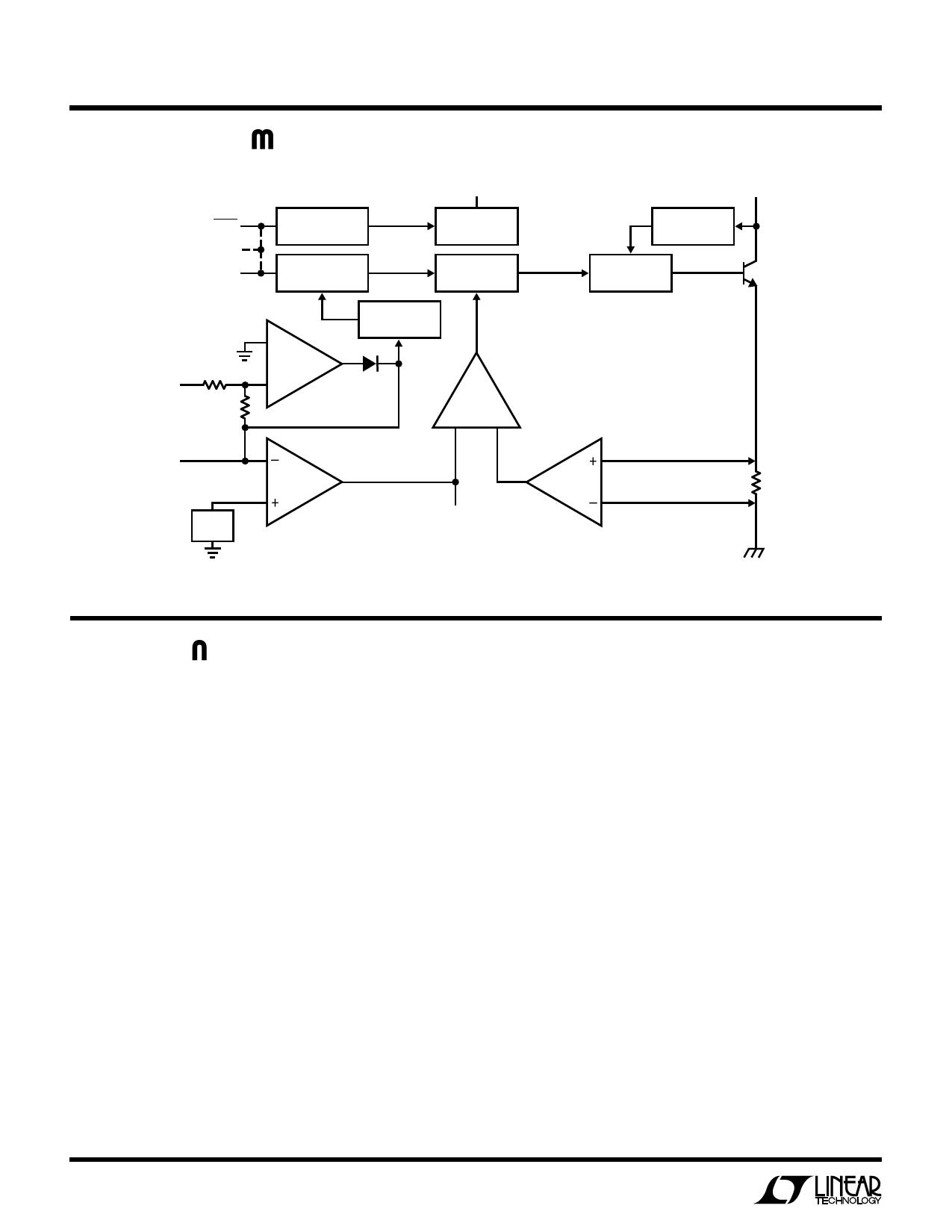
BLOCK DIAGRAM
SHDN
S/S*
SYNC
SHUTDOWN
DELAY AND RESET
SYNC
OSC
VIN
LOW DROPOUT
2.3V REG
LOGIC
100k
NFB
50k
+
NFBA
–
5:1 FREQUENCY
SHIFT
COMP
SW
ANTI-SAT
DRIVER
SWITCH
FB
1.245V
REF
GND SENSE
–
EA
+
IA
VC
AV ≈ 6
*R AND T7 PACKAGES ONLY
0.04Ω
GND LT1371 • BD
U
OPERATION
The LT1371 is a current mode switcher. This means that
switch duty cycle is directly controlled by switch current
rather than by output voltage. Referring to the block
diagram, the switch is turned ON at the start of each
oscillator cycle. It is turned OFF when switch current
reaches a predetermined level. Control of output voltage is
obtained by using the output of a voltage sensing error
amplifier to set current trip level. This technique has
several advantages. First, it has immediate response to
input voltage variations, unlike voltage mode switchers
which have notoriously poor line transient response.
Second, it reduces the 90° phase shift at mid-frequencies
in the energy storage inductor. This greatly simplifies
closed-loop frequency compensation under widely vary-
ing input voltage or output load conditions. Finally, it
allows simple pulse-by-pulse current limiting to provide
maximum switch protection under output overload or
short conditions. A low dropout internal regulator pro-
vides a 2.3V supply for all internal circuitry. This low
dropout design allows input voltage to vary from 2.7V to
25V with virtually no change in device performance. A
500kHz oscillator is the basic clock for all internal timing.
It turns ON the output switch via the logic and driver
circuitry. Special adaptive anti-sat circuitry detects onset
of saturation in the power switch and adjusts driver
current instantaneously to limit switch saturation. This
minimizes driver dissipation and provides very rapid turn-
off of the switch.
A 1.245V bandgap reference biases the positive input of
the error amplifier. The negative input of the amplifier is
brought out for positive output voltage sensing. The error
amplifier has nonlinear transconductance to reduce out-
put overshoot on start-up or overload recovery. When
the feedback voltage exceeds the reference by 40mV,
error amplifier transconductance increases 10 times,
which reduces output overshoot. The feedback input also
invokes oscillator frequency shifting, which helps pro-
tect components during overload conditions. When the
feedback voltage drops below 0.6V, the oscillator fre-
quency is reduced 5:1. Lower switching frequency allows
full control of switch current limit by reducing minimum
switch duty cycle.
6
Share Link: 