LT1619(RevA) データシートの表示(PDF) - Linear Technology
部品番号
コンポーネント説明
メーカー
LT1619 Datasheet PDF : 20 Pages
| |||
LT1619
APPLICATIO S I FOR ATIO
Diode
Schottky diodes are recommended for low output voltage
applications because of their low forward voltage. Since
Schottky diodes have negligible stored charge, charge
dumping loss is also reduced. The reverse breakdown
voltage of the diode should exceed the maximum reverse
voltage stress of the topology used. The diode should also
be able to carry the peak diode current with acceptable
foward voltage. For the boost converter in Figure 1, the
peak inductor current is approximately 5A. A Motorola
MBRD835 is used due to its low forward voltage.
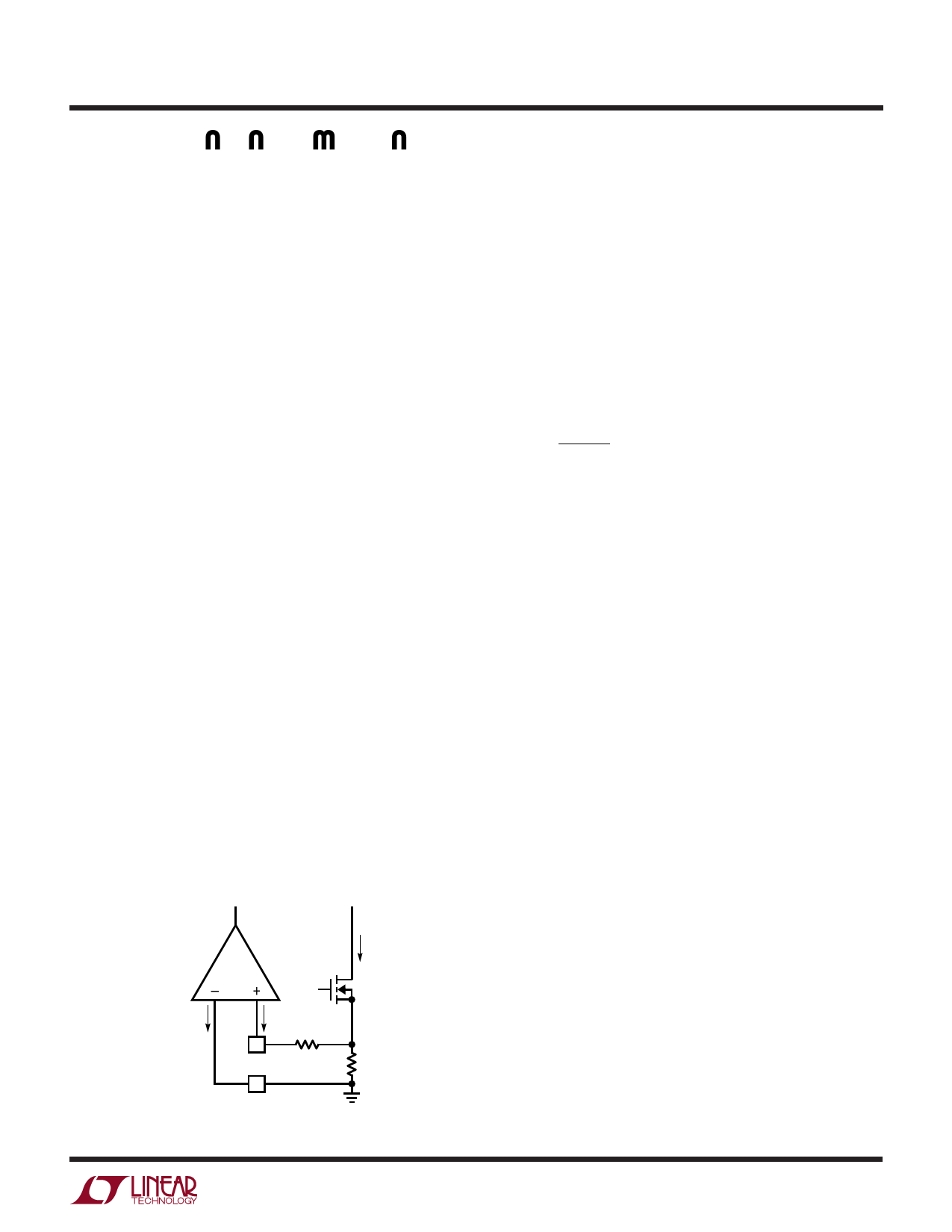
Lowering Burst Mode Operation Current Limit
The LT1619 automatically enters Burst Mode operation as
VC voltage falls below VB. The corresponding switch
current is the Burst Mode operation switch current thresh-
old, ID(BURST).
The effective Burst Mode operation current threshold can
be lowered by adding an offset to the input of the current
sense amplifier so that the switch current appears higher
to the PWM comparator. This has the effect of shifting the
VC operating range above VB. Although Burst Mode opera-
tion is not entirely disabled, the peak switch current before
entering Burst Mode operation is greatly reduced due to
the offset of the current sense amplifier. The peak switch
current is also determined by the current sense amplifier
blanking.
To lower the Burst Mode operation current sense thresh-
old, a resistor ROS is added between the SENSE pin and
the sense resistor RSENSE (Figure 5). The input bias
current IBIAS of the current sense amplifier, which has a
CURRENT
SENSE
ID
AMPLIFIER
IBIAS = 120µA
IBIAS = 120µA
5
SENSE
ROS
4
GND
RSENSE
1619 F05
Figure 5. Lowering Burst Mode Operation Current Limit
tolerance of ±25% and is temperature stable, develops an
offset voltage at the sense input. The value of ROS required
for non-Burst Mode operation can be obtained with the
expression:
IBIASROS ≥ VSENSE(BURST)
where
VSENSE(BURST) = (Burst Mode operation peak switch
current, ID(BURST)) • RSENSE
For example, if IBIAS = 120µA and VSENSE(BURST) = 10mV:
ROS
≥
10mV
120µA
=
83Ω
Allowing for 25% and 30% variations in IBAIS and
VSENSE(BURST) respectively:
ROS = (1.25)(1.3)(83Ω)
Choose ROS = 137Ω to completely disable Burst Mode
operation. Lower values of ROS (for example, 50Ω to
100Ω) can be used to lower the effective Burst Mode
current limit.
The value of the sense resistor is then adjusted to compen-
sate for the reduced full-scale sense voltage.
IBIASROS + IL(MAX)RSENSE = 40mV
Filtering Current Sense Signal
In a current mode converter, the current sense circuit
senses the switch current and terminates the switch
conduction. In the LT1619, the current sense amplifier
has a full-scale input voltage range from the ground to the
current limit threshold (53mV). Due to high speed switch-
ing transients and parasitic trace inductances, the current
sense signal VSENSE tends to be noisy. If the VSENSE
switching transient is excessive, the current sense ampli-
fier will amplify the spurious transient instead, resulting in
jittery operation. In situations where the internal leading
edge blanking is inadequate, a lowpass filter (Figure 6)
with corner frequency about 5 times the switching
frequency can be used to further attenuate high speed
switching transients. In Figure 6 the lowpass filter ROS and
CS has a corner frequency of:
1619fa
9
Share Link: 