LT1933HS6(RevD) データシートの表示(PDF) - Linear Technology
部品番号
コンポーネント説明
メーカー
LT1933HS6
(Rev.:RevD)
(Rev.:RevD)
Linear Technology

LT1933HS6 Datasheet PDF : 20 Pages
| |||
LT1933
PIN FUNCTIONS (SOT-23/DFN)
BOOST (Pin 1): The BOOST pin is used to provide a drive
voltage, higher than the input voltage, to the internal bipolar
NPN power switch.
GND (Pin 2/Pin 5 and Exposed Pad, Pin 7): Tie the
GND pin to a local ground plane below the LT1933 and
the circuit components. Return the feedback divider to
this pin.
FB (Pin 3/Pin 6): The LT1933 regulates its feedback pin to
1.245V. Connect the feedback resistor divider tap to this
pin. Set the output voltage according to VOUT = 1.245V
(1 + R1/R2). A good value for R2 is 10k.
SHDN (Pin 4): The SHDN pin is used to put the LT1933 in
shutdown mode. Tie to ground to shut down the LT1933.
Tie to 2.3V or more for normal operation. If the shutdown
feature is not used, tie this pin to the VIN pin. SHDN also
provides a soft-start function; see the Applications Infor-
mation section.
VIN (Pin 5/Pin 2): The VIN pin supplies current to the
LT1933’s internal regulator and to the internal power
switch. This pin must be locally bypassed.
SW (Pin 6): The SW pin is the output of the internal power
switch. Connect this pin to the inductor, catch diode and
boost capacitor.
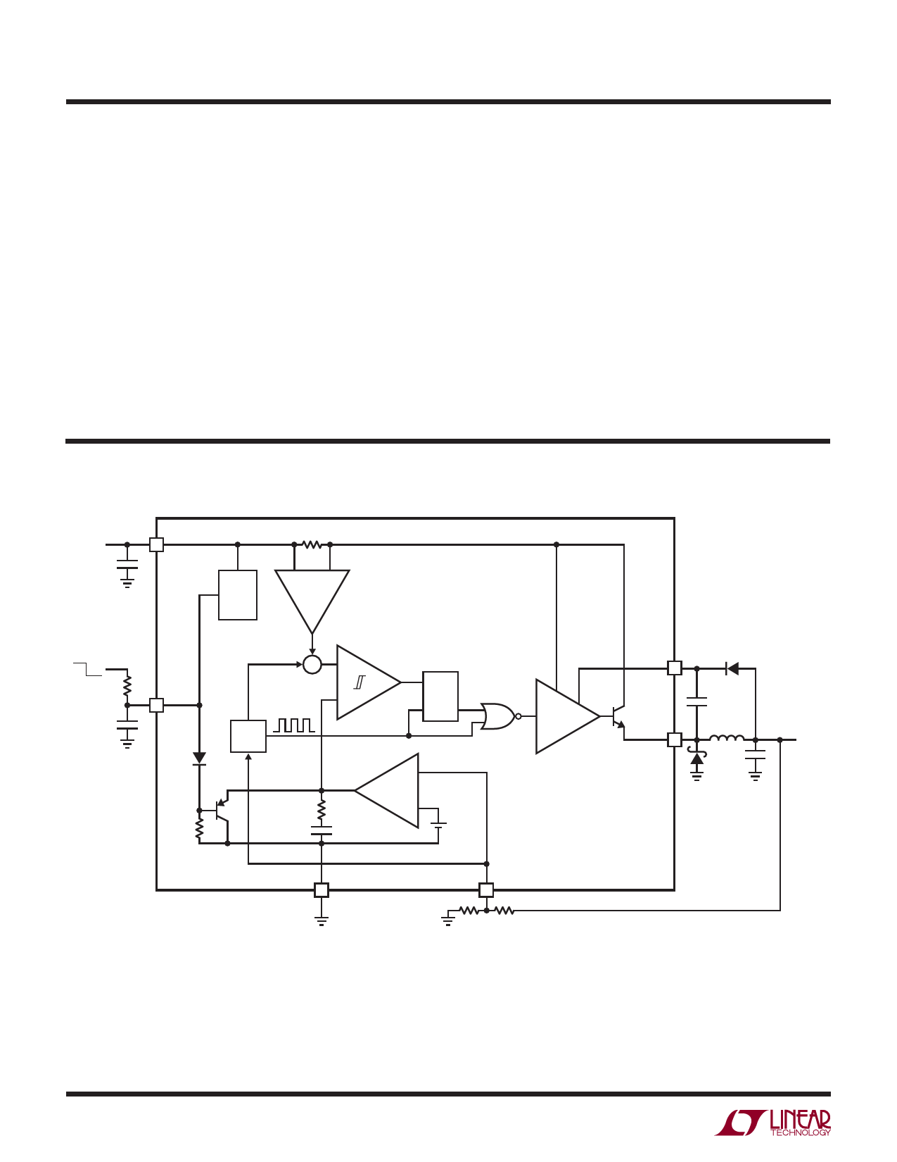
BLOCK DIAGRAM
VIN
VIN
C2
INT REG
AND
UVLO
ON OFF
R3
SHDN
C4
Σ
SLOPE
COMP
OSC
FREQUENCY
FOLDBACK
VC
RQ
SQ
gm
1.245V
DRIVER
BOOST
Q1
SW
D2
C3
L1
D1
VOUT
C1
GND
FB
R2
R1
1933 BD
1933fd
6
Share Link: