LT1950 データシートの表示(PDF) - Linear Technology
部品番号
コンポーネント説明
メーカー
LT1950 Datasheet PDF : 20 Pages
| |||
LT1950
APPLICATIO S I FOR ATIO
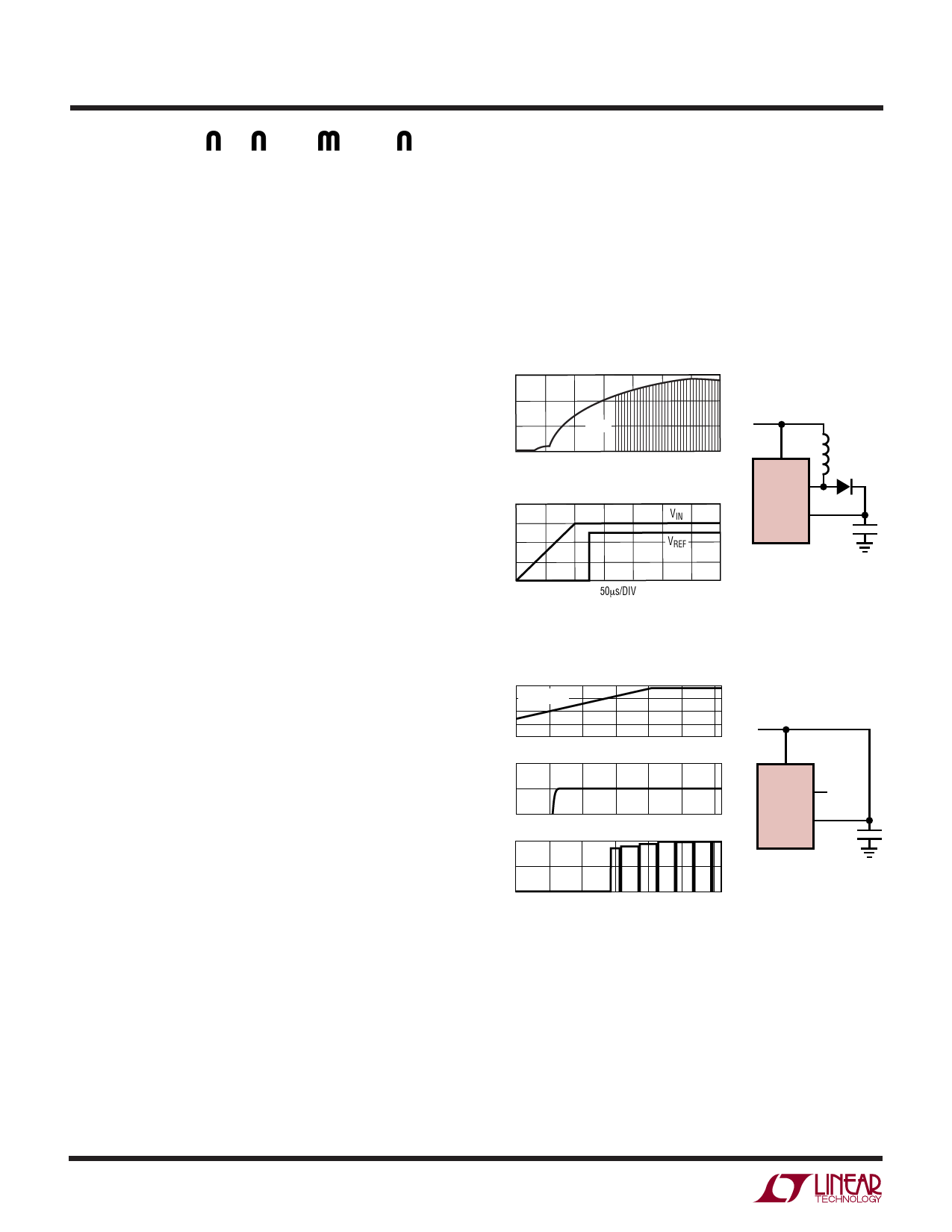
LT1950 Input Supplies, VREF Output and GATE Enable
VIN is the main input supply for the LT1950. VIN2 is the
input supply for the LT1950 output driver. VIN2 can be
provided by shorting the VIN2 pin to the VIN pin or by
generating VIN2 using the BOOST pin. Waveforms of VIN,
VIN2, VREF and GATE switching are shown in Figures 2 and
3. Figure 2 represents low VIN operation with VIN2 gener-
ated using the B00ST pin. Figure 3 represents VIN = VIN2
operation with the BOOST pin open circuit or shorted to
ground.
Low VIN Operation
The LT1950 can be configured to provide a minimum of
10V GATE drive for an external N-channel MOSFET from
VIN voltages as low as 3V, if the BOOST pin is used to
generate a second supply at the VIN2 pin (see Figure 2 and
Applications Information “ Generating VIN2 Supply Using
BOOST Pin”). The advantage of this configuration is that a
lower RDS(ON) is achieved for the external N-channel
MOSFET, improving efficiency, versus a controller run-
ning at 3V input without boosted gate drive. In addition,
typical controllers running at low input voltages have the
limitation of only being able to use logic level MOSFETs.
The LT1950 allows a greater range of usable MOSFETs.
This versatility allows optimization of the overall power
supply performance and allows applications which would
otherwise not be possible without a more complex topol-
ogy. Figure 2 shows that for VIN above 2V, the internal
switcher at the BOOST pin is enabled. This switch gener-
ates the VIN2 supply. As VIN2 ramps up above the
undervoltage lockout threshold of 6.8V the 2.5V reference
VREF becomes active and powers up internal control
circuitry. When VIN2 exceeds approximately 8V, the gate
driver is enabled. VIN2 is regulated between 10V and 11V,
providing a supply to the LT1950 output driver to ensure
a minimum of 10V drive at the GATE pin.
VIN = VIN2 Operation
If low VIN operation is not required below approximately
8V on VIN the LT1950 can be configured to run without the
use of the BOOST pin by shorting the VIN2 pin to the VIN
pin. Figure 3 shows that both VIN and VIN2 must now
exceed 6.8V to activate the 2.5V VREF output and must
exceed approximately 8V to enable the output driver
(GATE pin).
12
8
VIN2
MIN
4
GATE
3V
0
L1
VIN
D1
BOOST
4
LT1950
3
VIN
VIN2
C1
2
VREF
1
0
50µs/DIV
1950 F02
Figure 2. Low VIN Operation
10.2
8.5 VIN = VIN2
6.8
5.1
3.4
5.0
VREF
2.5
0
10
GATE
5
0
TYPICAL START-UP INPUT
>8.2V
VIN
BOOST
LT1950
VIN2
*
C1
10µs/DIV
*BOOST PIN CAN BE
LEFT OPEN OR
SHORTED TO GROUND
1950 F03
Figure 3. VIN = VIN2 Operation
1950fa
10
Share Link: 