3433EFE データシートの表示(PDF) - Linear Technology
部品番号
コンポーネント説明
メーカー
3433EFE Datasheet PDF : 16 Pages
| |||
LT3433
APPLICATIO S I FOR ATIO
The requirement for avoiding current mode instability is
that the rising slope of sensed inductor ripple current (S1)
is greater than the falling slope (S2). At duty cycles greater
than 50% this is not true. To avoid the instability condition,
a false signal is added to the sensed current with a slope
(SX) that is sufficient to prevent current mode instability,
or S1 + SX ≥ S2. This leads to the following relations:
SX ≥ S2(2DC – 1)/DC
If the forward voltages of a converter’s catch and pass
diodes are defined as VF1 and VF2, then:
S2 = (VOUT + VF1 + VF2)/L
Solving for L yields a relation for the minimum inductance
that will satisfy slope compensation requirements:
LMIN = (VOUT + VF1 + VF2)(2DC – 1)/(DC • SX)
The LT3433 maximizes available dynamic range using a
slope compensation generator that generates a continu-
ously increasing slope as duty cycle increases. The slope
compensation waveform is calibrated at 80% duty cycle to
generate an equivalent slope of at least 0.05A/µs. The
equation for minimum inductance then reduces to:
LMIN = (VOUT + VF1 + VF2)(15e-6)
For example, with VOUT = 5V and using VF1 + VF2 = 1.1V
(cold):
LMIN = (5 + 1.1)(15e-6) = 91.5µH
Converter Capabilities
The output current capability of an LT3433 converter is
affected by a myriad of variables. The current in the
switches is limited by the LT3433. Switch current is
measured coming from the VIN supply, and does not
directly translate to a limitation in load current. This is
especially true during bridged mode operation when the
converter output current is discontinuous.
During bridged mode operation, the converter output
current is discontinuous, or only flowing to the output
while the switches are off (not to be confused with discon-
tinuous switcher operation). As a result, the maximum
output current capability of the converter is reduced from
that during buck mode operation by a factor of roughly
1 – DC, not including additional losses. Most converter
losses are also a function of DC, so operational duty cycle
must be accurately determined to predict converter load
capabilities.
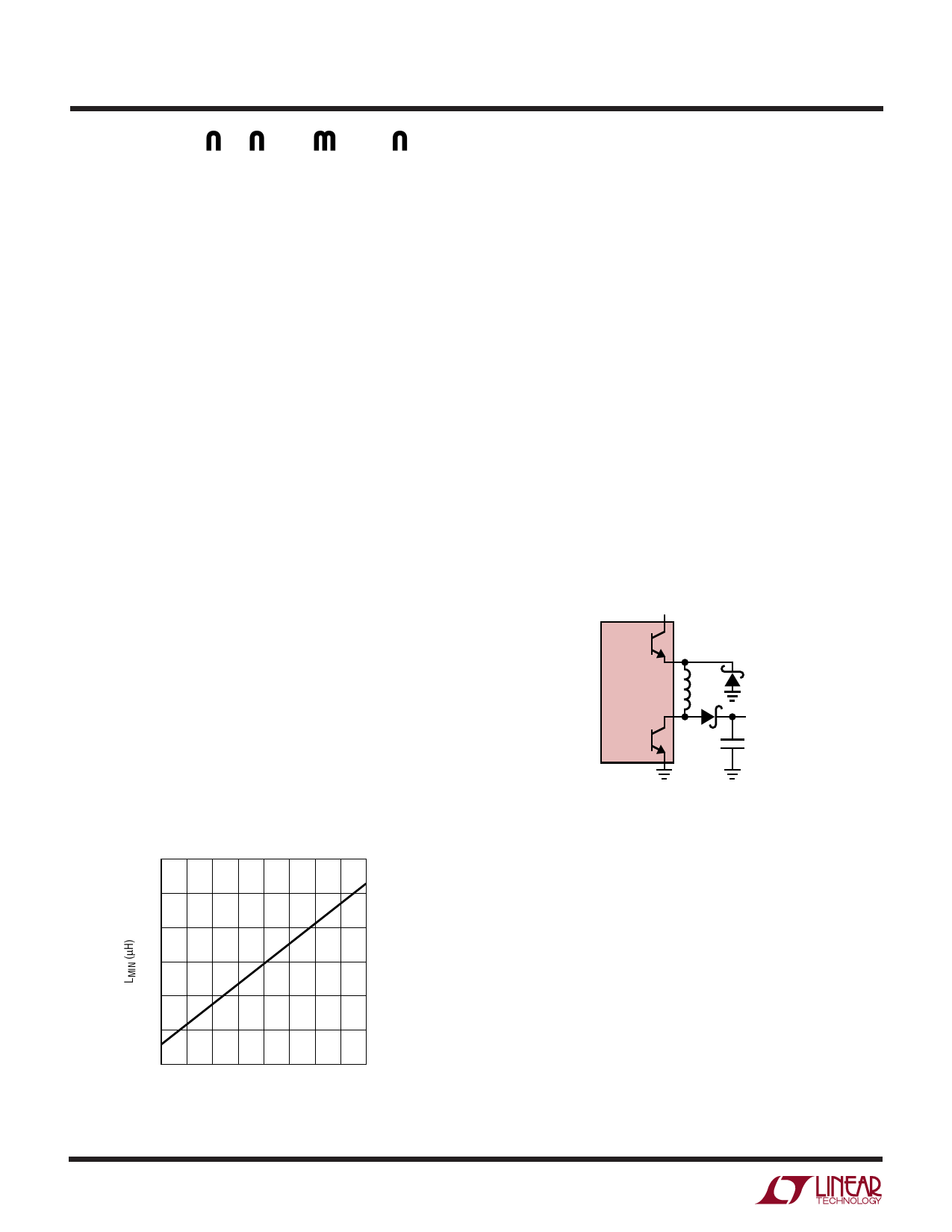
VIN
SW_H
LT3433
SW_L
L
D2
D1
VOUT
3433 AI02
Slope Compensation Requirements
Typical Minimum Inductor Values vs VOUT
350
300
250
200
150
100
50
4 6 8 10 12 14 16 18 20
VOUT (V)
3433 AI01
10
Application variables:
VIN = Converter input supply voltage
VOUT = Converter programmed output voltage
VBST = Boosted supply voltage (VBST – VSWH)
DC = Operational duty cycle
fO = Switching frequency
IMAX = Peak switch current limit
∆IL = Inductor ripple current
ISW = Average switch current or peak switch current
less half the ripple current (IMAX – ∆IL/2)
RSWH = Boosted switch “on” resistance
RSWL = Grounded switch “on” resistance
L = Inductor value
3433f
Share Link: 