LT3470 データシートの表示(PDF) - Linear Technology
部品番号
コンポーネント説明
メーカー
LT3470 Datasheet PDF : 20 Pages
| |||
LT3470
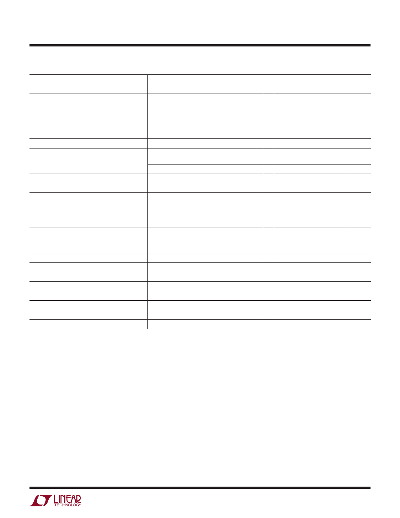
Electrical Characteristics The l denotes the specifications which apply over the full operating
temperature range, otherwise specifications are at TA = 25°C. VIN = 10V, VSHDN = 10V, VBOOST = 15V, VBIAS = 3V unless otherwise specified.
PARAMETER
CONDITIONS
MIN TYP MAX
UNITS
Minimum Input Voltage
●
4
V
Quiescent Current from VIN
Quiescent Current from Bias
FB Comparator Trip Voltage
FB Pin Bias Current (Note 3)
VSHDN = 0.2V
VBIAS = 3V, Not Switching
VBIAS = 0V, Not Switching
VSHDN = 0.2V
VBIAS = 3V, Not Switching
VBIAS = 0V, Not Switching
VFB Falling
VFB = 1V, E- and I-Grade
0.1
0.5
µA
●
10
18
µA
35
50
µA
0.1
0.5
µA
●
25
60
µA
0.1
1.5
µA
● 1.228 1.250 1.265
V
35
80
nA
●
35
150
nA
H-Grade
●
35
225
nA
FB Voltage Line Regulation
Minimum Switch Off-Time (Note 5)
4V < VIN < 40V
0.0006 0.01
%/V
500
ns
Switch Leakage Current
0.7
1.5
µA
Switch VCESAT
Switch Top Current Limit
Switch Bottom Current Limit
Catch Schottky Drop
Catch Schottky Reverse Leakage
Boost Schottky Drop
Boost Schottky Reverse Leakage
Minimum Boost Voltage (Note 4)
ISW = 100mA (TS8 Package)
ISW = 100mA (DD8 Package)
VFB = 0V
VFB = 0V
ISH = 100mA (TS8 Package)
ISH = 100mA (DD8 Package)
VSW = 10V
ISH = 30mA
VSW = 10V, VBIAS = 0V
215
300
mV
215
mV
250
325
435
mA
225
mA
630
775
mV
630
mV
0.2
2
µA
650
775
mV
0.2
2
µA
●
1.7
2.2
V
BOOST Pin Current
SHDN Pin Current
SHDN Input Voltage High
ISW = 100mA
VSHDN = 2.5V
7
12
mA
1
5
µA
2.5
V
SHDN Input Voltage Low
0.2
V
Note 1: Stresses beyond those listed under Absolute Maximum Ratings
may cause permanent damage to the device. Exposure to any Absolute
Maximum Rating condition for extended periods may affect device
reliability and lifetime.
Note 2: The LT3470E is guaranteed to meet performance specifications
from 0°C to 85°C. Specifications over the –40°C to 85°C operating
temperature range are assured by design, characterization and
correlation with statistical process controls. The LT3470I specifications
are guaranteed over the –40°C to 125°C temperature range. LT3470H
specifications are guaranteed over –40°C to 150°C temperature range.
Note 3: Bias current flows out of the FB pin.
Note 4: This is the minimum voltage across the boost capacitor needed to
guarantee full saturation of the switch.
Note 5: This parameter is assured by design and correlation with statistical
process controls.
3470fd
3
Share Link: 