LT3470E データシートの表示(PDF) - Linear Technology
部品番号
コンポーネント説明
メーカー
LT3470E Datasheet PDF : 20 Pages
| |||

LT3470
Applications Information
Input Voltage Range
The minimum input voltage required to generate a par-
ticular output voltage in an LT3470 application is limited
by either its 4V undervoltage lockout or by its maximum
duty cycle. The duty cycle is the fraction of time that the
internal switch is on and is determined by the input and
output voltages:
DC = VOUT + VD
VIN – VSW + VD
where VD is the forward voltage drop of the catch diode
(~0.6V) and VSW is the voltage drop of the internal switch
at maximum load (~0.4V). Given DCMAX = 0.90, this leads
to a minimum input voltage of:
VIN(MIN)
=
VOUT + VD
DCMAX
+
VSW
–
VD
This analysis assumes the part has started up such that the
capacitor tied between the BOOST and SW pins is charged
to more than 2V. For proper start-up, the minimum input
voltage is limited by the boost circuit as detailed in the
section BOOST Pin Considerations.
The maximum input voltage is limited by the absolute
maximum VIN rating of 40V, provided an inductor of suf-
ficient value is used.
Inductor Selection
The switching action of the LT3470 during continuous
operation produces a square wave at the SW pin that
results in a triangle wave of current in the inductor. The
hysteretic mode control regulates the top and bottom
current limits (see Electrical Characteristics) such that
the average inductor current equals the load current. For
safe operation, it must be noted that the LT3470 cannot
turn the switch on for less than ~150ns. If the inductor is
small and the input voltage is high, the current through the
switch may exceed safe operating limit before the LT3470
is able to turn off. To prevent this from happening, the
following equation provides a minimum inductor value:
LMIN
=
VIN(MAX )
• tON-TIME(MIN)
IMAX
where VIN(MAX) is the maximum input voltage for the ap-
plication, tON-TIME(MIN) is ~150ns and IMAX is the maximum
allowable increase in switch current during a minimum
switch on-time (150mA). While this equation provides a
safe inductor value, the resulting application circuit may
switch at too high a frequency to yield good efficiency.
It is advised that switching frequency be below 1.2MHz
during normal operation:
f = (1– DC)(VD + VOUT )
L • ∆IL
where f is the switching frequency, ∆IL is the ripple current
in the inductor (~150mA), VD is the forward voltage drop
of the catch diode, and VOUT is the desired output voltage.
If the application circuit is intended to operate at high duty
cycles (VIN close to VOUT), it is important to look at the
calculated value of the switch off-time:
tOFF -TIME
=
1– DC
f
The calculated tOFF-TIME should be more than LT3470’s
minimum tOFF-TIME (See Electrical Characteristics), so
the application circuit is capable of delivering full rated
output current. If the full output current of 200mA is not
required, the calculated tOFF-TIME can be made less than
minimum tOFF-TIME possibly allowing the use of a smaller
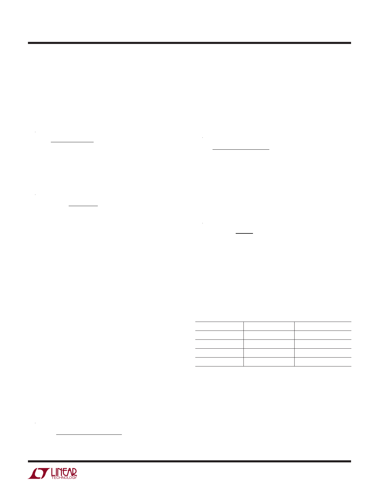
inductor. See Table 1 for an inductor value selection guide.
Table 1. Recommended Inductors for Loads up to 200mA
VOUT
VIN UP TO 16V
VIN UP TO 40V
2.5V
10µH
33µH
3.3V
10µH
33µH
5V
15µH
33µH
12V
33µH
47µH
Choose an inductor that is intended for power applications.
Table 2 lists several manufacturers and inductor series.
For robust output short-circuit protection at high VIN (up
to 40V) use at least a 33µH inductor with a minimum
450mA saturation current. If short-circuit performance is
not required, inductors with ISAT of 300mA or more may
3470fd
9