LT3475IFE-PBF データシートの表示(PDF) - Linear Technology
部品番号
コンポーネント説明
メーカー
LT3475IFE-PBF Datasheet PDF : 20 Pages
| |||
LT3475/LT3475-1
APPLICATIONS INFORMATION
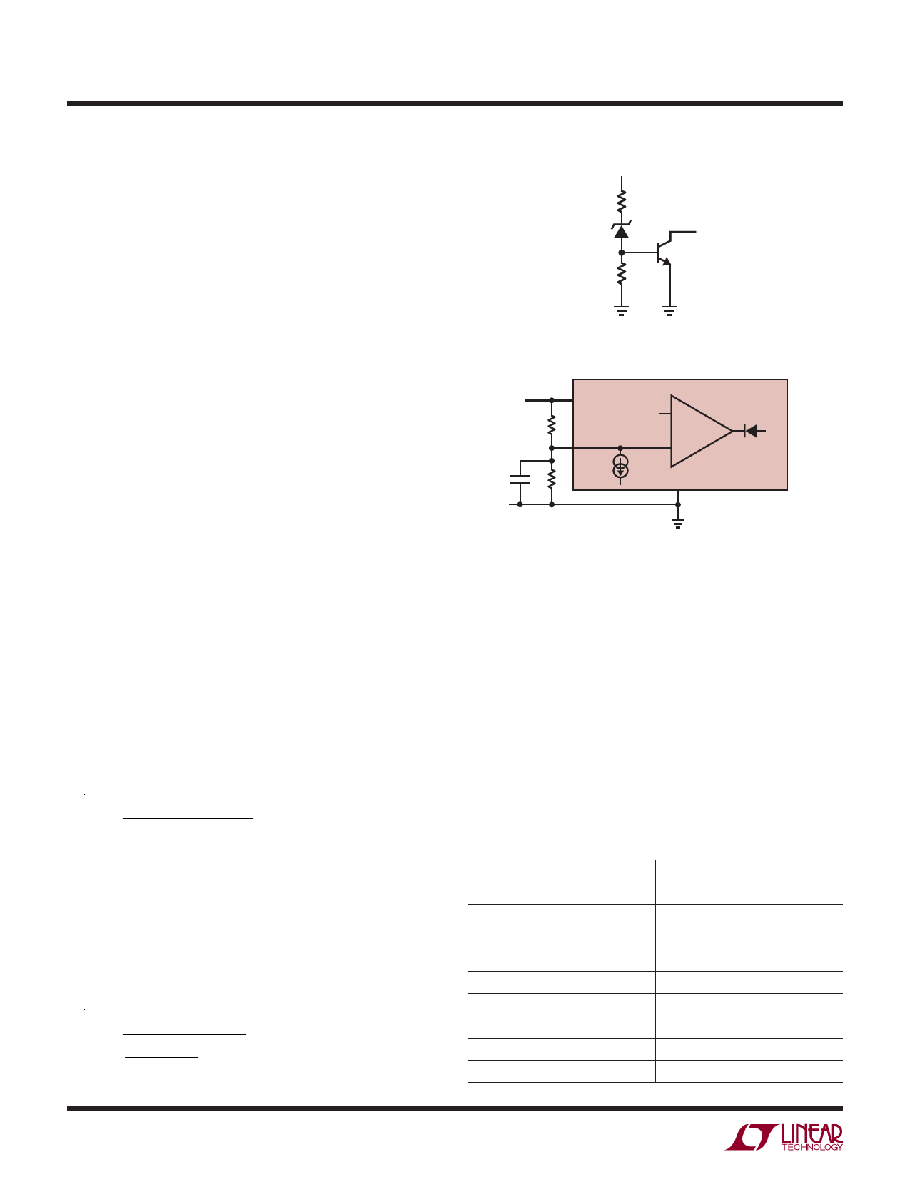
Open Circuit Protection
The LT3475 has internal open-circuit protection. If the LED
is absent or is open circuit, the LT3475 clamps the voltage
on the LED pin at 14V. The switching regulator then oper-
ates at a very low frequency to limit the input current. The
LT3475-1 has no internal open circuit protection. With the
LT3475-1, be careful not to violate the ABSMAX voltage of
th BOOST pin; if VIN > 25V, external open circuit protection
circuitry (as shown in Figure 1) may be necessary.The
output voltage during an open LED condition is shown in
the Typical Performance Characteristics section.
Undervoltage Lockout
Undervoltage lockout (UVLO) is typically used in situations
where the input supply is current limited, or has high source
resistance. A switching regulator draws constant power
from the source, so the source current increases as the
source voltage drops. This looks like a negative resistance
load to the source and can cause the source to current limit
or latch low under low source voltage conditions. UVLO
prevents the regulator from operating at source voltages
where these problems might occur.
An internal comparator will force the part into shut-
down when VIN falls below 3.7V. If an adjustable UVLO
threshold is required, the SHDN pin can be used. The
threshold voltage of the SHDN pin comparator is 2.6V. An
internal resistor pulls 9μA to ground from the SHDN pin
at the UVLO threshold.
Choose resistors according to the following formula:
2.6V
R2 =
VT H
– 2.6V
R1
– 9μA
VTH = UVLO Threshold
Example: Switching should not start until the input is
above 8V.
VTH = 8V
R1=100k
R2 =
2.6V
8V – 2.6V
100k
–
9μA
=
57.6k
8
OUT
10k
22V
VC
100k
3475 F01
Figure 1. External Overvoltage Protection
Circuitry for the LT3475-1
VIN
VIN
R1
SHDN
C1 R2
2.6V
9μA
GND
LT3475
VC
3475 F02
Figure 2. Undervoltage Lockout
Keep the connections from the resistors to the SHDN pin
short and make sure the coupling to the SW and BOOST
pins is minimized. If high resistance values are used, the
SHDN pin should be bypassed with a 1nF capacitor to
prevent coupling problems from switching nodes.
Setting the Switching Frequency
The LT3475 uses a constant frequency architecture that
can be programmed over a 200kHz to 2MHz range with a
single external timing resistor from the RT pin to ground.
A graph for selecting the value of RT for a given operating
frequency is shown in the Typical Applications section.
Table 1. Switching Frequencies
SWITCHING FREQUENCY (MHz)
RT (kΩ)
2
4.32
1.5
6.81
1.2
9.09
1
11.8
0.8
16.9
0.6
24.3
0.4
40.2
0.3
57.6
0.2
100
3475fb
Share Link: 