LT3475IFE-PBF データシートの表示(PDF) - Linear Technology
部品番号
コンポーネント説明
メーカー
LT3475IFE-PBF Datasheet PDF : 20 Pages
| |||
LT3475/LT3475-1
APPLICATIONS INFORMATION
Table 1 shows suggested RT selections for a variety of
switching frequencies.
Operating Frequency Selection
The choice of operating frequency is determined by
several factors. There is a tradeoff between efficiency and
component size. A higher switching frequency allows the
use of smaller inductors at the cost of increased switching
losses and decreased efficiency.
Another consideration is the maximum duty cycle. In certain
applications, the converter needs to operate at a high duty
cycle in order to work at the lowest input voltage possible.
The LT3475 has a fixed oscillator off time and a variable
on time. As a result, the maximum duty cycle increases
as the switching frequency is decreased.
Input Voltage Range
The minimum operating voltage is determined either by the
LT3475’s undervoltage lockout of 4V, or by its maximum
duty cycle. The duty cycle is the fraction of time that the
internal switch is on and is determined by the input and
output voltages:
DC
=
(VOUT +
(VIN – VSW
VF
+
)
VF
)
where VF is the forward voltage drop of the catch diode
(~0.4V) and VSW is the voltage drop of the internal switch
(~0.4V at maximum load). This leads to a minimum input
voltage of:
VIN(MIN)
=
VOUT + VF
DCMAX
–
VF
+ VSW
with DCMAX = 1–tOFF(MIN) • f
where t0FF(MIN) is equal to 167ns and f is the switching
frequency.
Example: f = 600kHz, VOUT = 4V
DCMAX = 1− 167ns • 600kHz = 0.90
VIN(MIN)
=
4V
+ 0.4V
0.9
–
0.4V
+
0.4V
=
4.9V
The maximum operating voltage is determined by the
absolute maximum ratings of the VIN and BOOST pins,
and by the minimum duty cycle.
VIN(MAX )
=
VOUT + VF
DCMIN
–
VF
+
VSW
with DCMIN = tON(MIN) • f
where tON(MIN) is equal to 140ns and f is the switching
frequency.
Example: f = 750kHz, VOUT = 3.4V
DCMIN = 140ns • 750kHz = 0.105
VIN(MAX
)
=
3.4V + 0.4V
0.105
–
0.4V
+
0.4V
=
36V
The minimum duty cycle depends on the switching fre-
quency. Running at a lower switching frequency might
allow a higher maximum operating voltage. Note that
this is a restriction on the operating input voltage; the
circuit will tolerate transient inputs up to the Absolute
Maximum Ratings of the VIN and BOOST pins. The input
voltage should be limited to the VIN operating range (36V)
during overload conditions (short circuit or start up).
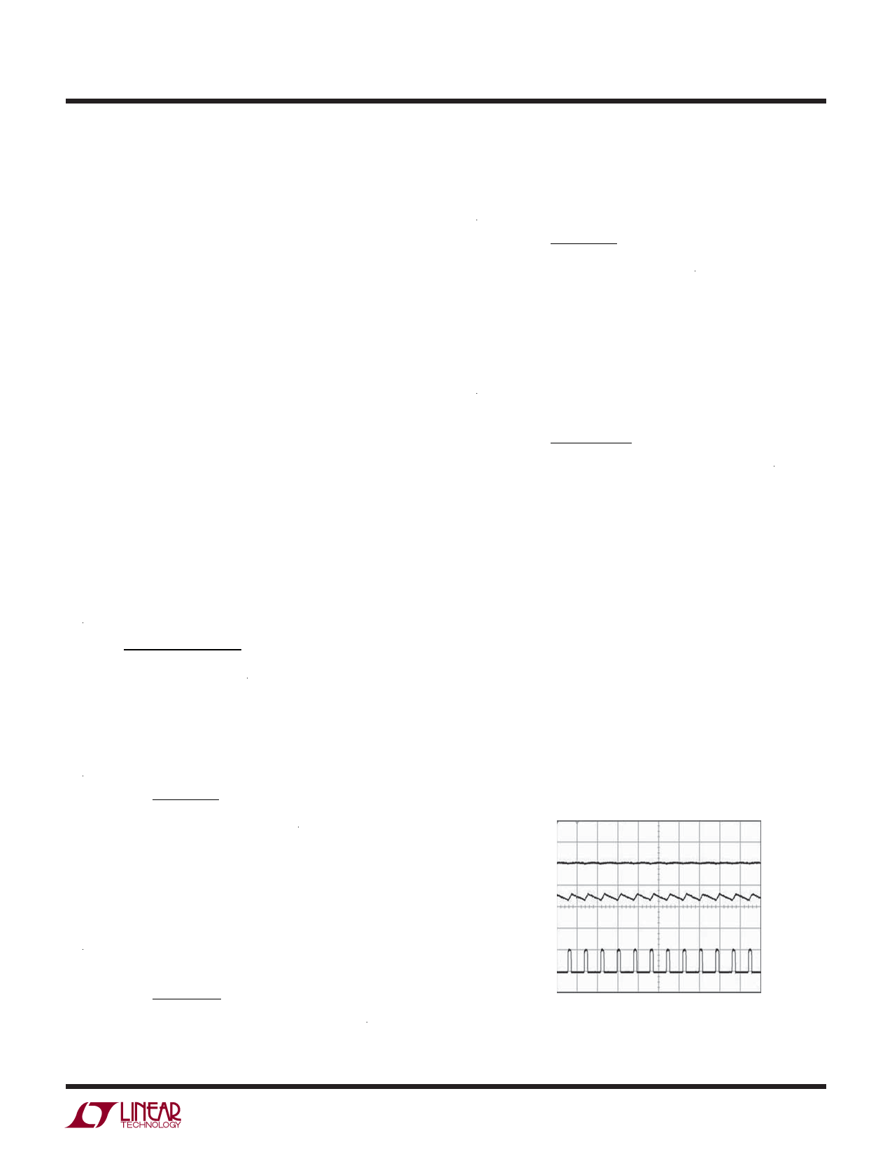
Minimum On Time
The LT3475 will regulate the output current at input volt-
ages greater than VIN(MAX). For example, an application
with an output voltage of 3V and switching frequency of
1.2MHz has a VIN(MAX) of 20V, as shown in Figure 3. Figure
4 shows operation at 35V. Output ripple and peak inductor
VOUT
500mV/DIV
(AC COUPLED)
IL
1A/DIV
VSW
20V/DIV
3475 F03
Figure 3. Operation at VIN(MAX) = 20V.
VOUT = 3V and fSW = 1.2MHHz
3475fb
9
Share Link: 