LT3510FE(RevC) データシートの表示(PDF) - Linear Technology
部品番号
コンポーネント説明
メーカー
LT3510FE Datasheet PDF : 28 Pages
| |||
TYPICAL PERFORMANCE CHARACTERISTICS
LT3510
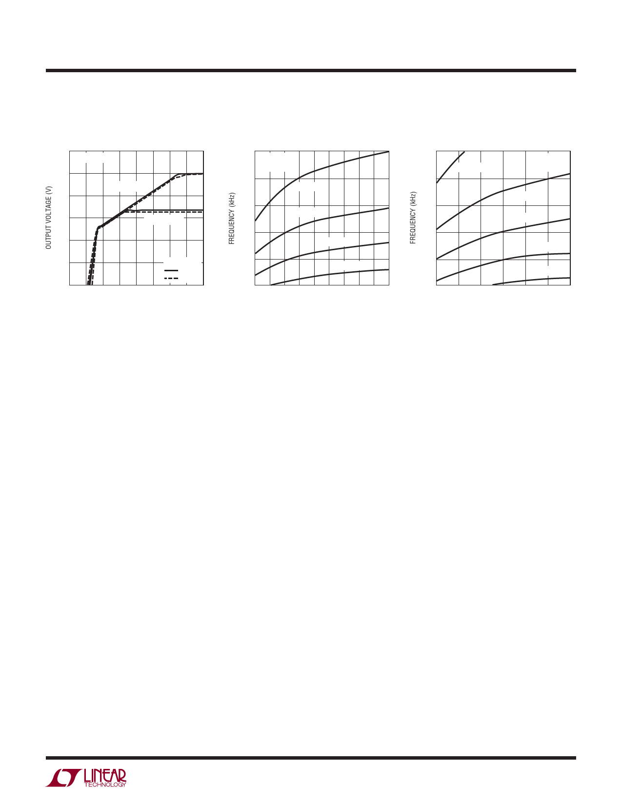
Dropout Operation
6
LOAD = 1A
5
VOUT = 5V
4
3
VOUT = 3.3V
2
1
FREQUENCY
1.5MHz
250kHz
0
2 2.5 3 3.5 4 4.5 5 5.5 6
INPUT VOLTAGE (V)
3510 G27
Inductor Value vs Frequency for
2A Maximum Load Current
1500
VOUT = 3.3V
IRIPPLE = 1A
1250
L = 2.2μH
1000
L = 3.3μH
750
L = 4.7μH
500
L = 6.8μH
250
7 9 11 13 15 17 19 21 23 25
INPUT VOLTAGE (V)
3510 G28
Inductor Value vs Frequency for
2A Maximum Load Current
1500
L = 2.2μH
VOUT = 5V
IRIPPLE = 1A
1250
1000
750
500
250
10
L = 3.3μH
L = 4.7μH
L = 6.8μH
L = 10μH
12.5 15 17.5 20
INPUT VOLTAGE (V)
22.5 25
3510 G29
PIN FUNCTIONS
VIN1 (Pin 1): The VIN1 pin powers the internal control
circuitry for both channels and is monitored by the
undervoltage lockout comparator. The VIN1 pin is also
connected to the collector of channel 1’s on-chip power
NPN switch. The VIN1 pin has high dI/dt edges and must
be decoupled to ground close to the pin of the device.
SW1/SW2 (Pins 2, 9): The SW pin is the emitter of the on-
chip power NPN. At switch off, the inductor will drive this
pin below ground with a high dV/dt. An external Schottky
catch diode to ground, close to the SW pin and respective
VIN decoupling capacitor’s ground, must be used to prevent
this pin from excessive negative voltages.
IND1/IND2 (Pins 3, 8): The IND pin is the input to the
on-chip sense resistor that measures current flowing in
the inductor. When the current in the resistor exceeds
the current dictated by the VC pin, the SW latch is held in
reset, disabling the output switch. Bias current flows out
of the IND pin when IND is less than 1.6V.
VOUT1/VOUT2 (Pins 4, 7): The VOUT pin is the output to
the on-chip sense resistor that measures current flowing
in the inductor. When the current in the resistor exceeds
the current dictated by the VC pin, the SW latch is held in
reset, disabling the output switch. Bias current flows out
of the VOUT pin when VOUT is less than 1.6V.
PG1/PG2 (Pins 5, 6): The power good pin is an open-col-
lector output that sinks current when the feedback falls
below 90% of its nominal regulating voltage. For VIN1
above 1V, its output state remains true, although during
shutdown, VIN1 undervoltage lockout or thermal shutdown,
its current sink capability is reduced. The PG pins can be
left open circuit or tied together to form a single power
good signal.
VIN2 (Pin 10): The VIN2 pin is the collector of channel 2’s
on-chip power NPN switch. This pin is independent of VIN1
and may be connected to the same or a separate supply. In
either case, high dI/dt edges are present and decoupling
to ground must be used close to this pin.
SS1/SS2 (Pins 19, 12): The SS1/2 pins control the soft-
start and sequence of their respective outputs. A single
capacitor from the SS pin to ground determines the outpt
ramp rate. For soft-start and output tracking/sequencing
details, see the Applications Information section.
VC1/VC2 (Pins 18, 13): The VC pin is the output of the
error amplifier and the input to the peak switch current
comparator. It is normally used for frequency compensa-
tion, but can also be used as a current clamp or control
loop override. If the error amplifier drives VC above the
maximum switch current level, a voltage clamp activates.
3510fc
7
Share Link: 