LT3510FE データシートの表示(PDF) - Linear Technology
部品番号
コンポーネント説明
メーカー
LT3510FE Datasheet PDF : 30 Pages
| |||
LT3510
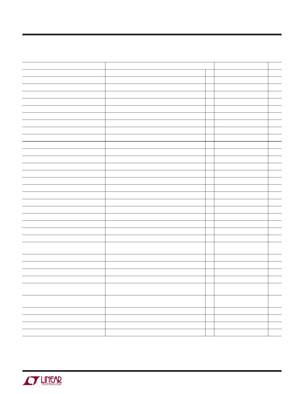
ELECTRICAL CHARACTERISTICS The l denotes the specifications which apply over the full operating
temperature range, otherwise specifications are at TJ = 25°C. VVIN1/2 = 15V, VBST1/2 = open, VRT/SYNC = 2V, VVOUT1/2 = open,
unless otherwise specified.
PARAMETER
CONDITIONS
Feedback Voltage Line Regulation
VVIN1/2 = 3V to 25V
Feedback Voltage Offset Ch 1 to Ch 2
Feedback Bias Current Ch 1/Ch 2
Error Amplifier gm Ch 1/Ch 2
Error Amplifier Gain Ch 1/Ch 2
VVC1/2 = 1V
VFB1/2 = 0.8V, VVC1/2 = 1V
VVC1/2 = 1V, IVC1/2 = ±5μA
Error Amplifier to Switch Gain Ch 1/Ch 2
Error Amplifier Source Current Ch 1/Ch 2
VFB1/2 = 0.6V, VVC1/2 = 1V
Error Amplifier Sink Current Ch 1/Ch 2
Error Amplifier High Clamp Ch 1/Ch 2
Error Amplifier Switching Threshold Ch 1/Ch 2
Soft-Start Source Current Ch 1/Ch 2
Soft-Start VOH Ch 1/Ch 2
Soft-Start Sink Current Ch 1/Ch 2
VFB1/2 = 1V, VVC1/2 = 1V
VFB1/2 = 0.7V
VOUT1/2 = 5V, RT/SYNC = 133k
VFB1/2 = 0.6V, VSS1/2 = 0.4V
VFB1/2 = 0.9V
VFB1/2 = 0.6V, VSS1/2 = 1V
Soft-Start VOL Ch 1/Ch 2
Soft-Start to Feedback Offset Ch 1/Ch 2
Soft-Start Sink Current Ch 1/Ch 2 POR
Soft-Start POR Threshold Ch 1/Ch 2
Soft-Start Switching Threshold Ch 1/Ch 2
Power Good Leakage Ch 1/Ch 2
Power Good Threshold Ch 1/Ch 2
Power Good Hysteresis Ch 1/Ch 2
Power Good Sink Current Ch 1/Ch 2
Power Good Shutdown Sink Current Ch 1/Ch 2
RT/SYNC Reference Voltage
VFB1/2 = 0V
VVC1/2 = 1V, VSS1/2 = 0.4V
VSS1/2 = 0.4V (Note 4), VVC = 1V
VFB1/2 = 0V (Note 4)
VFB1/2 = 0V
VFB1/2 = 0.9V, VPG1/2 = 25V, VVIN1/2 = 25V, VOUT = 5V
VFB1/2 Rising, PG1/2 = 20k to 5V
VFB1/2 Falling, PG1/2 = 20k to 5V
VFB1/2 = 0.65V, VPG1/2 = 0.4V
VVIN1/2 = 2V, VFB1/2 = 0V, VPG1/2 = 0.4V
VFB1/2 = 0.9V, IRT/SYNC = –40μA
Switching Frequency
Switching Phase Angle Ch A to Ch B
RT/SYNC = 133k, VFB1/2 = 0.6V, VBST1/2 = VSW + 3V
RT/SYNC = 15.4k, VFB1/2 = 0.6V, VBST1/2 = VSW + 3V
RT/SYNC = 133k, VFB1/2 = 0.6V, VBST1/2 = VSW + 3V
Minimum Boost for 100% Duty Cycle Ch 1/Ch 2
SYNC Frequency Range
SYNC Switching Phase Angle Ch A to Ch B
IND + VOUT Current Ch 1/Ch 2
IND to VOUT Maximum Current Ch 1/Ch 2
Switch Leakage Current Ch 1/Ch 2
Switch Saturation Voltage Ch 1/Ch 2
Boost Current Ch 1/Ch 2
VFB1/2 = 0.7V, IRT/SYNC = –35μA (Note 5), VOUT = 0V
VBST1/2 = VSW + 3V
SYNC = 250kHz, VBST1/2 = VSW + 3V
VVOUT1/2 = 0V, VFB1/2 = 0.9V
VVOUT1/2 = 5V
VVOUT1/2 = 0.5V (Note 6), VFB1/2 = 0.7V, VBST1/2 = 20V
VVOUT1/2 = 5V (Note 6), RT/SYNC = 133k, VBST1/2 = 20V
VSW1/2 = 0V, VVIN1/2 = 25V
ISW1/2 = 2A, VBST1/2 = 20V, VFB1/2 = 0.7V
ISW1/2 = 2A, VBST1/2 = 20V, VFB1/2 = 0.7V
Minimum Boost Voltage Ch 1/Ch 2
ISW1/2 = 2A, VBST1/2 = 20V, VFB1/2 = 0.7V (Note 7)
MIN
l –1
l –16
l –200
l 150
10
15
1.75
0.5
l
2
1.9
200
50
l –16
0.5
55
30
l 87
20
400
10
0.93
200
1.2
120
250
120
40
2.25
2.5
l
l
25
TYP
0
0
75
275
1000
2.2
15
20
2.0
0.7
3
2
600
80
0
1.5
80
50
0
90
30
800
50
0.975
250
1.5
180
1.7
180
70
0
2.8
2.8
0
250
50
1.4
MAX UNITS
1
%
16
mV
200
nA
450 μmho
V/V
A/V
25
μA
30
μA
2.25
V
1.0
V
4.2
μA
2.4
V
1000
μA
125
mV
16
mV
2
mA
105
mV
70
mV
1
μA
93
%
50
mV
1200
μA
100
μA
1
V
300
kHz
1.8
MHz
210
Deg
2
V
1500
kHz
210
Deg
100
μA
1
μA
4
A
4
A
50
μA
400
mV
100
mA
2.5
V
Note 1: Stresses beyond those listed under Absolute Maximum Ratings
may cause permanent damage to the device. Exposure to any Absolute
Maximum Rating condition for extended periods may affect device
reliability and lifetime.
Note 2: The LT3510EFE is guaranteed to meet performance specifications
from 0°C to 125°C junction temperature. Specifications over the –40°C
to 125°C operating junction temperature range are assured by design,
characterization and correlation with statistical process controls. The
3510fe
3
Share Link: 