LT3510EFE-TRPBF データシートの表示(PDF) - Linear Technology
部品番号
コンポーネント説明
メーカー
LT3510EFE-TRPBF Datasheet PDF : 30 Pages
| |||
LT3510
ELECTRICAL CHARACTERISTICS
LT3510IFE is guaranteed and tested over the full –40°C to 125°C operating
junction temperature range.
Note 3: Minimum input voltage is defined as the voltage where internal
bias lines are regulated so that the reference voltage and oscillator remain
constant. Actual minimum input voltage to maintain a regulated output
will depend upon output voltage and load current. See Applications
Information.
Note 4: An internal power-on reset (POR) latch is set on the positive
transition of the SHDN pin through its threshold. The output of the latch
activates current sources on each SS pin which typically sink 1.5mA,
discharging the SS capacitor. The latch is reset when both SS pins are
driven below the soft-start POR threshold or the SHDN pin is taken below
its threshold.
Note 5: To enhance dropout operation, the output switch will be turned off
for the minimum off time only when the voltage across the boost capacitor
drops below the minimum boost for 100% duty cycle threshold.
Note 6: The IND to VOUT maximum current is defined as the value of
current flowing from the IND pin to the VOUT pin which resets the switch
latch when the VC pin is at its high clamp.
Note 7: This is the minimum voltage across the boost capacitor needed to
guarantee full saturation of the internal power switch.
Note 8: This IC includes overtemperature protection that is intended
to protect the device during momentary overload conditions. Junction
temperature will exceed 125°C when overtemperature protection is active.
Continuous operation above the specified maximum operating junction
temperature may impair device reliability.
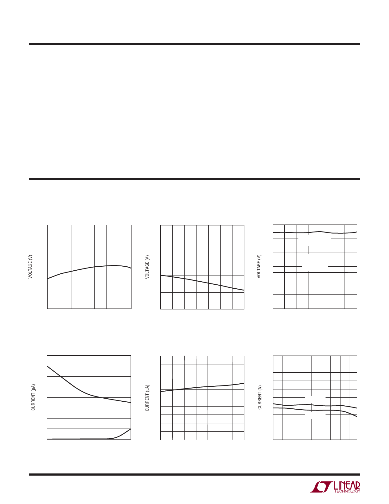
TYPICAL PERFORMANCE CHARACTERISTICS
Feedback Voltage vs Temperature
0.816
0.811
0.806
0.801
0.796
0.791
0.786
–50 –25
0 25 50 75
TEMPERATURE (°C)
100 125
3510 G02
Shutdown Quiescent Current
vs Temperature
16
14
VVIN1
12
10
8
6
4
2
0
–50 –25
VVIN2
0 25 50 75
TEMPERATURE (°C)
100 125
3510 G05
RT/SYNC Voltage vs Temperature
1.05
1.03
1.01
0.99
0.97
0.95
–50 –25
0 25 50 75
TEMPERATURE (°C)
100 125
3510 G03
Soft-Start Source Current
vs Temperature
4.0
3.8
3.6
3.4
3.2
3.0
2.8
2.6
2.4
2.2
2.0
–50 –25
0 25 50 75
TEMPERATURE (°C)
100 125
3510 G07
4
Shutdown Threshold and Minimum
Input Voltage vs Temperature
3.0
2.5
MINIMUM INPUT
VOLTAGE
2.0
SHUTDOWN
THRESHOLD
1.5
VOLTAGE
1.0
0.5
0
–50 –25
0 25 50 75
TEMPERATURE (°C)
100 125
3510 G04
IND to VOUT Maximum Current vs
Temperature
4.0
3.8
3.6
3.4
3.2
3.0
VOUT = 5V
2.8
2.6
VOUT = 0V
2.4
2.2
2.0
–50 –30 –10 10 30 50 70 90 110
TEMPERATURE (°C)
3510 G30
3510fe
Share Link: 