LT3581IMSE-TRPBF データシートの表示(PDF) - Linear Technology
部品番号
コンポーネント説明
メーカー
LT3581IMSE-TRPBF Datasheet PDF : 36 Pages
| |||
LT3581
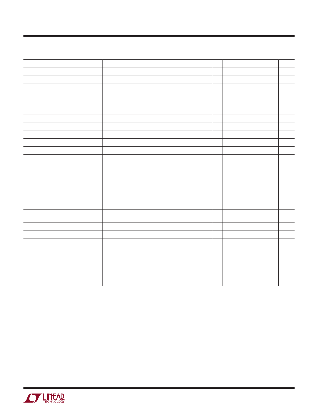
ELECTRICAL CHARACTERISTICS The l denotes the specifications which apply over the full operating
temperature range, otherwise specifications are at TA = 25°C. VIN = 5V, VSHDN = VIN, VFAULT = VIN, unless otherwise noted. (Note 2).
PARAMETER
CONDITIONS
MIN TYP MAX UNITS
Minimum Input Voltage
l
2.3
2.5
V
VIN Overvoltage Lockout
Positive Feedback Voltage
22.1 23.5
25
V
l 1.195 1.215 1.230
V
Negative Feedback Voltage
l
3
9
16
mV
Positive FB Pin Bias Current
VFB = Positive Feedback Voltage, Current into Pin
l 81
83.3
85
µA
Negative FB Pin Bias Current
Error Amp Transconductance
VFB = Negative Feedback Voltage, Current out of Pin
ΔI = 10μA
l 81
83.3 85.5
µA
270
µmhos
Error Amp Voltage Gain
70
V/V
Quiescent Current
Not Switching
1.9
2.3
mA
Quiescent Current in Shutdown
VSHDN = 0V
0
1
µA
Reference Line Regulation
Switching Frequency, fOSC
2.5V ≤ VIN ≤ 20V
RT = 34k
RT = 432k
0.01 0.05
%/V
l 2.25
2.5
2.75
MHz
l 180
200
220
kHz
Switching Frequency in Foldback
Compared to Normal fOSC
1/6
ratio
Switching Frequency Range
Free-Running or Synchronizing
l 200
2500
kHz
SYNC High Level for Synchronization
l 1.3
V
SYNC Low Level for Synchronization
l
0.4
V
SYNC Clock Pulse Duty Cycle
VSYNC = 0V to 2V
20
80
%
Recommended Minimum SYNC Ratio
fSYNC/fOSC
Minimum Off-Time
3/4
45
ns
Minimum On-Time
55
ns
SW1 Current Limit
At All Duty Cycles
l 1.9
2.4
3
A
Current Sharing (SW2/SW1)
78
%
SW1 + SW2 Current Limit
At All Duty Cycles, SW2/SW1 = 78% (Note 3)
l 3.3
4.3
5.4
A
Switch VCESAT
SW1 & SW2 Tied Together, ISW1 + ISW2 = 2.75A
250
mV
SW1 Leakage Current
SW2 Leakage Current
VSW1 = 5V
VSW2 = 5V
0.01
1
µA
0.01
1
µA
For more information www.linear.com/LT3581
3581fb
3
Share Link: 