LT5520EUF データシートの表示(PDF) - Linear Technology
部品番号
コンポーネント説明
メーカー
LT5520EUF Datasheet PDF : 12 Pages
| |||
LT5520
APPLICATIO S I FOR ATIO
100Ω
C1
0.1%
18mA
T1
2
IFIN
4:1
50Ω
C3
VCC
3
C2
100Ω
18mA
0.1% LT5520
5520 F03
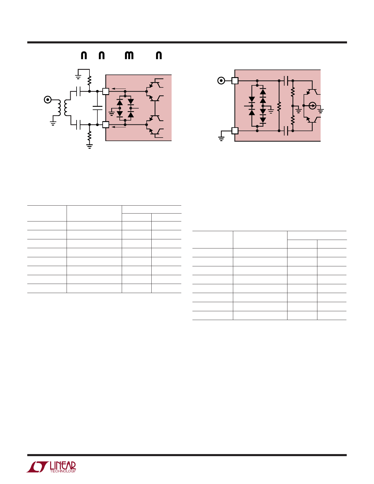
Figure 3. IF Input with External Matching
LOIN
50Ω
LO+
14
5pF
220Ω
VCC
85Ω
15 LO–
LT5520
5pF 220Ω
5520 F04
Figure 4. LO Input Circuit
Table 1 lists the differential IF input impedance and reflec-
tion coefficient for several frequencies. A 4:1 balun can be
used to transform the impedance up to about 50Ω.
Table 1. IF Input Differential Impedance
Frequency
(MHz)
Differential Input
Impedance
Differential S11
Mag
Angle
10
10.1 + j0.117
0.663
180
44
10.1 + j0.476
0.663
179
70
10.1 + j0.751
0.663
178
140
10.2 + j1.47
0.663
177
170
10.2 + j1.78
0.663
176
240
10.2 + j2.53
0.663
174
360
10.2 + j3.81
0.663
171
500
10.2 + j5.31
0.663
167
LO Input Port
The simplified circuit for the LO buffer input is shown in
Figure 4. The LO buffer amplifier consists of high-speed
limiting differential amplifiers, optimized to drive the mixer
quad for high linearity. The LO+ and LO– ports can be
driven differentially; however, they are intended to be
driven by a single-ended source. An internal resistor
connected across the LO+ and LO– inputs provides a
broadband 50Ω impedance match. Because of the resis-
tive match, a DC voltage at the LO input is not recom-
mended. If the LO signal source output is not AC coupled,
then a DC blocking capacitor should be used at the LO
input.
Though the LO input is internally 50Ω matched, there may
be some cases, particularly at higher frequencies or with
different source impedances, where a further optimized
match is desired. Table 2 includes the single -ended input
impedance and reflection coefficient vs frequency for the
LO input for use in such cases.
Table 2. Single-Ended LO Input Impedance
Frequency
(MHz)
Input
Impedance
S11
Mag
Angle
1300
62.8 – j9.14
0.139
– 30.9
1500
62.2 – j11.4
0.148
– 37.1
1700
61.5 – j13.4
0.157
– 42.4
1900
60.0 – j15.2
0.164
– 48.9
2100
58.4 – j16.9
0.172
– 54.7
2300
56.5 – j17.9
0.176
– 60.4
2500
54.9 – j18.8
0.182
– 65.1
2700
53.7 – j18.8
0.182
– 68.5
RF Output Port
An internal RF transformer, shown in Figure 5, reduces the
mixer-core impedance to provide an impedance of 50Ω
across the RF + and RF – pins. The LT5520 is designed and
tested with the outputs configured for single-ended opera-
tion, as shown in the Figure 5; however, the outputs can be
used differentially as well. A center-tap in the transformer
provides the DC connection to the mixer core and the
transformer provides DC isolation at the RF output. The
RF+ and RF– pins are connected together through the
secondary windings of the transformer, thus a DC voltage
should not be applied across these pins.
5520f
7
Share Link: 