LT5520 データシートの表示(PDF) - Linear Technology
部品番号
コンポーネント説明
メーカー
LT5520 Datasheet PDF : 12 Pages
| |||
LT5520
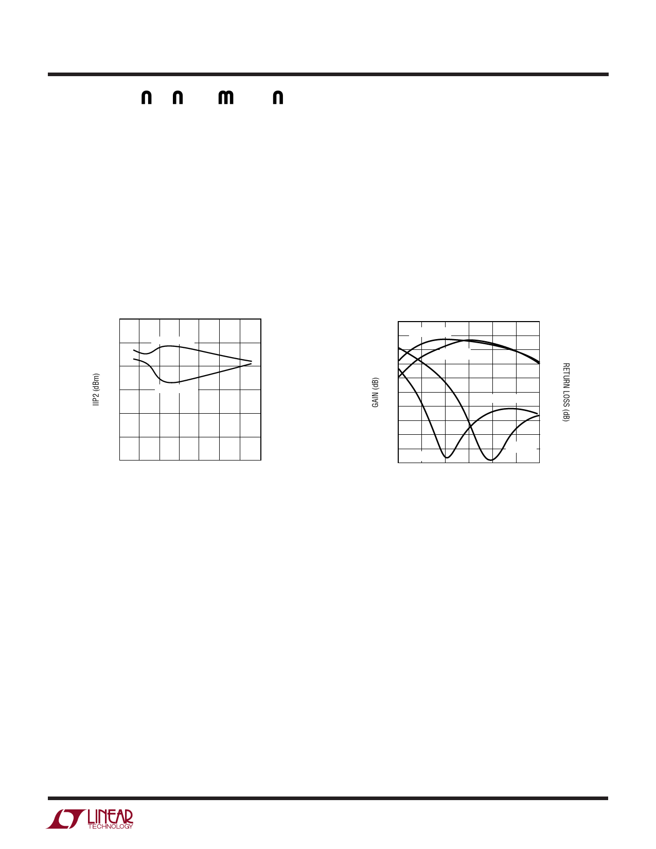
APPLICATIO S I FOR ATIO
Figures 6-8 illustrate the performance versus tuned IF
input frequency with both high side and low side LO
injection. Figure 6 shows the measured conversion gain
and IIP3. The noise figure is plotted in Figure 7 for LO
power levels of –5dBm and 0dBm. At lower input frequen-
cies, the LO power level has little impact on noise figure.
However, for higher frequencies, an increased LO drive
level may be utilized to achieve better noise figure. The
single-tone IIP2 behavior is illustrated in Figure 8.
60
50
LOW SIDE LO
40
30
HIGH SIDE LO
20
10
0
0 100 200 300 400 500 600 700
INPUT FREQUENCY (MHz)
5520 F08
Figure 8. IIP2 vs Tuned IF Input Frequency
Low Frequency Matching of the RF Output Port
Without any external components on the RF output, the
internal transformer of the LT5520 provides a good 50Ω
impedance match for RF frequencies above approximately
1600MHz. At frequencies lower than this, the return loss
drops below 10dB and degrades the conversion gain. The
addition of a single 3.3pF capacitor in series with the RF
output improves the match at lower RF frequencies,
shifting the 10dB return loss point to about 1300MHz, as
demonstrated in Figure 9. This change also results in an
improvement of the conversion gain, as shown in
Figure 9.
1
0
0
COUT = 3.3pF
–1
NO COUT
GAIN
–5
–2
–3
–10
–4
RETURN LOSS
–5
–15
–6
–7
–20
–8
COUT = 3.3pF
–9
1200 1400 1600
1800
2000
FREQUENCY (MHz)
NO COUT
–25
2200 2400
5520 F09
Figure 9. Conversion Gain and Return Loss vs Output Frequency
5520f
9
Share Link: 