LTC1258-2.5 データシートの表示(PDF) - Linear Technology
部品番号
コンポーネント説明
メーカー
LTC1258-2.5 Datasheet PDF : 8 Pages
| |||
LTC1258 Series
APPLICATIONS INFORMATION
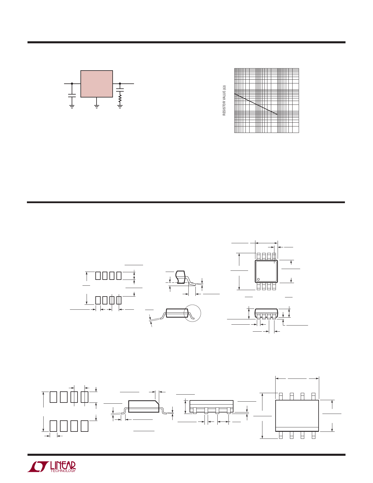
5.2V
TO
12.6V
0.1μF
LTC1258-5
2
IN
1
OUT
GND
4
5V
COUT
>1μF
DAMPING RESISTOR
<1k
1258 F02
Figure 2. Adding a Damping Resistor with
Output Capacitors Greater Than 1μF
Internal P-Channel Pass Transistor
The LTC1258 series features an internal P-channel MOSFET
pass transistor. This provides several advantages over
similar designs using a PNP bipolar pass transistor.
These references consume only 4μA of quiescent current
under light and heavy loads as well as in dropout; whereas,
10k
1k
100
10
1
10
100
1000
OUTPUT CAPACITOR VALUE (μF)
1258 F03
Figure 3. Damping Resistance vs Output Capacitor Value
PNP-based references waste considerable amounts of
current when the pass transistor is saturated. In addition,
the LTC1258 series provides a lower dropout voltage
(200mV max) than PNP-based references.
PACKAGE DESCRIPTION
MS8 Package
8-Lead Plastic MSOP
(Reference LTC DWG # 05-08-1660 Rev F)
3.00 p 0.102
(.118 p .004)
(NOTE 3)
8 7 65
0.52
(.0205)
REF
0.889 p 0.127
(.035 p .005)
0.254
(.010)
DETAIL “A”
0o – 6o TYP
4.90 p 0.152
(.193 p .006)
3.00 p 0.102
(.118 p .004)
(NOTE 4)
5.23
(.206)
MIN
GAUGE PLANE
3.20 – 3.45
(.126 – .136)
0.53 p 0.152
(.021 p .006)
DETAIL “A”
1 234
1.10
(.043)
MAX
0.86
(.034)
REF
0.42 p 0.038
0.65
0.18
(.0165 p .0015)
TYP
(.0256)
BSC
(.007)
SEATING
RECOMMENDED SOLDER PAD LAYOUT
PLANE
0.22 – 0.38
(.009 – .015)
TYP
0.65
(.0256)
0.1016 p 0.0508
(.004 p .002)
MSOP (MS8) 0307 REV F
NOTE:
BSC
1. DIMENSIONS IN MILLIMETER/(INCH)
4. DIMENSION DOES NOT INCLUDE INTERLEAD FLASH OR PROTRUSIONS.
2. DRAWING NOT TO SCALE
INTERLEAD FLASH OR PROTRUSIONS SHALL NOT EXCEED 0.152mm (.006") PER SIDE
3. DIMENSION DOES NOT INCLUDE MOLD FLASH, PROTRUSIONS OR GATE BURRS.
5. LEAD COPLANARITY (BOTTOM OF LEADS AFTER FORMING) SHALL BE 0.102mm (.004") MAX
MOLD FLASH, PROTRUSIONS OR GATE BURRS SHALL NOT EXCEED 0.152mm (.006") PER SIDE
S8 Package
8-Lead Plastic Small Outline (Narrow .150 Inch)
(Reference LTC DWG # 05-08-1610)
.050 BSC
.045 p.005
.010 – .020 s 45o
(0.254 – 0.508)
.053 – .069
(1.346 – 1.752)
.008 – .010
(0.203 – 0.254)
0o– 8o TYP
.245
MIN
.160 p.005
.030 p.005
TYP
.016 – .050
(0.406 – 1.270)
NOTE:
1. DIMENSIONS
IN
INCHES
(MILLIMETERS)
.014 – .019
(0.355 – 0.483)
TYP
2. DRAWING NOT TO SCALE
3. THESE DIMENSIONS DO NOT INCLUDE MOLD FLASH OR PROTRUSIONS.
RECOMMENDED SOLDER PAD LAYOUT
MOLD FLASH OR PROTRUSIONS SHALL NOT EXCEED .006" (0.15mm)
.004 – .010
(0.101 – 0.254)
.050
(1.270)
BSC
.228 – .244
(5.791 – 6.197)
.189 – .197
(4.801 – 5.004)
NOTE 3
8
7
6
5
1
2
34
.150 – .157
(3.810 – 3.988)
NOTE 3
SO8 0303
1258sfb
Information furnished by Linear Technology Corporation is believed to be accurate and reliable.
However, no responsibility is assumed for its use. Linear Technology Corporation makes no representa-
tion that the interconnection of its circuits as described herein will not infringe on existing patent rights.
7
Share Link: 