LTC1650ACN(1999) データシートの表示(PDF) - Linear Technology
部品番号
コンポーネント説明
メーカー
LTC1650ACN Datasheet PDF : 12 Pages
| |||
LTC1650
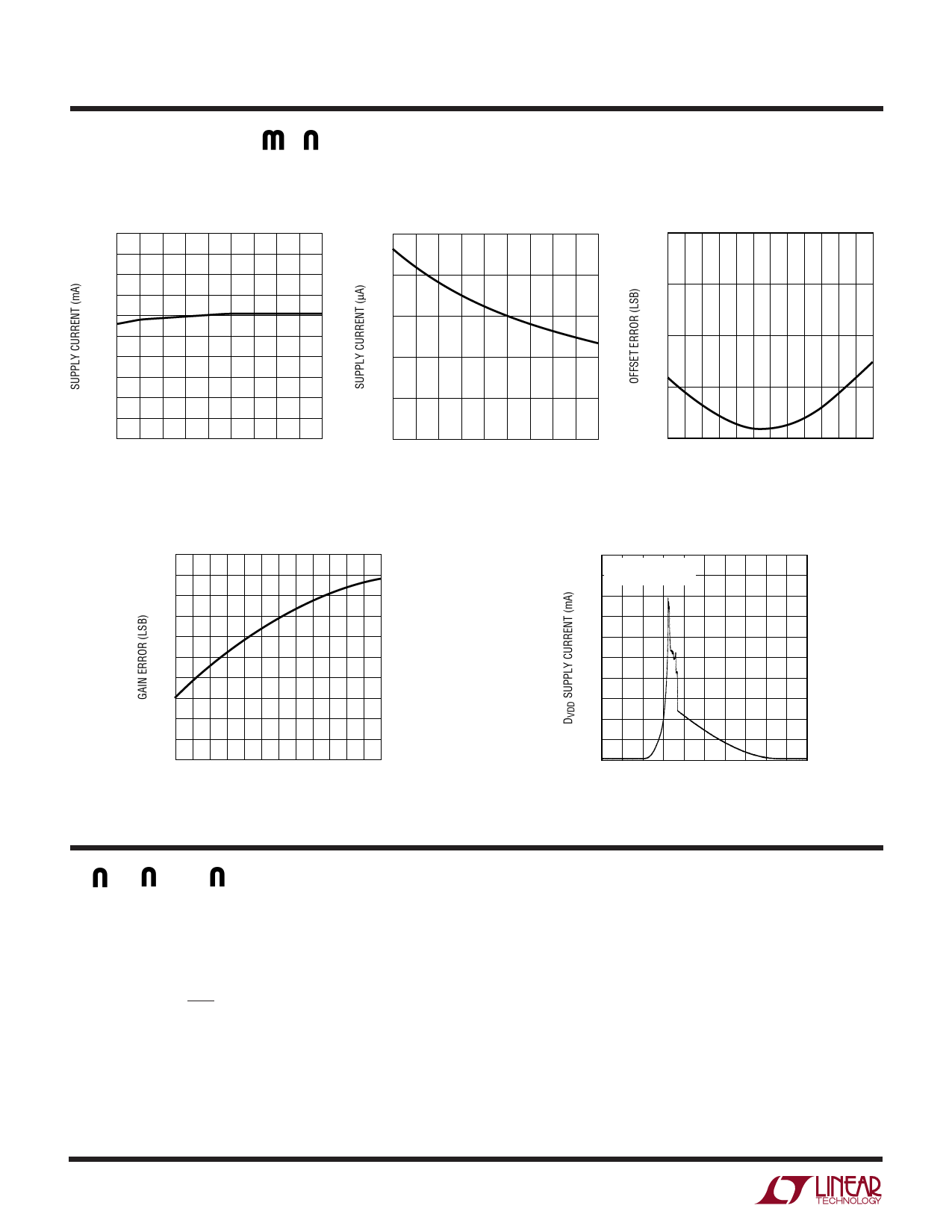
TYPICAL PERFOR A CE CHARACTERISTICS
AVSS Supply Current vs
Temperature
–4.5
–4.6
–4.7
–4.8
–4.9
–5.0
–5.1
–5.2
–5.3
–5.4
–5.5
–55 –35 –15 5 25 45 65 85 105 125
TEMPERATURE (°C)
1650 G10
DVDD Supply Current vs
Temperature
25
20
15
10
5
0
–55 –35 –15 5 25 45 65 85 105 125
TEMPERATURE (°C)
1650 G11
Offset Error vs Temperature
0
–0.5
–1.0
–1.5
–2.0
–55
–25 5 35 65
TEMPERATURE (°C)
95 125
1650 G12
Gain Error vs Temperature
0
–1
–2
–3
–4
–5
–6
–7
–8
–9
–10
–55 –25 5
35 65 95 125
TEMPERATURE (°C)
1650 G13
Supply Current vs Logic Input
Voltage
2
ALL LOGIC INPUTS
TIED TOGETHER
1
0
0
1
2
3
4
5
LOGIC INPUT VOLTAGE (V)
1650 G14
PIN FUNCTIONS
VOUT (Pin 1): The Rail-to-Rail Deglitched DAC Output.
The output will swing from REFLO to REFHI in unipolar
mode and from (2 • REFLO – REFHI) to REFHI in bipolar
mode.
VRST (Pin 2): The user-defined voltage to which the output
gets reset when CLR is active, when any of the supplies
drop below 2.5V or when the part powers-up. The output
will stay at this voltage until a new code is loaded into the
DAC register.
DVDD (Pin 3): The Digital Positive Supply Input. 4.75V ≤
DVDD ≤ 5.25V.
DGND (Pin 4): Digital Ground.
DIN (Pin 5): The TTL Level Input for the Serial Interface
Data. Data on the DIN pin is latched into the shift register
on the rising edge of the serial clock. Data is loaded as one
16-bit word, MSB first.
DOUT (Pin 6): The output of the shift register that be-
comes valid on the rising edge of the serial clock.
6
Share Link: 