LTC1726IS8-2.5(RevB) データシートの表示(PDF) - Linear Technology
部品番号
コンポーネント説明
メーカー
LTC1726IS8-2.5
(Rev.:RevB)
(Rev.:RevB)
Linear Technology

LTC1726IS8-2.5 Datasheet PDF : 12 Pages
| |||
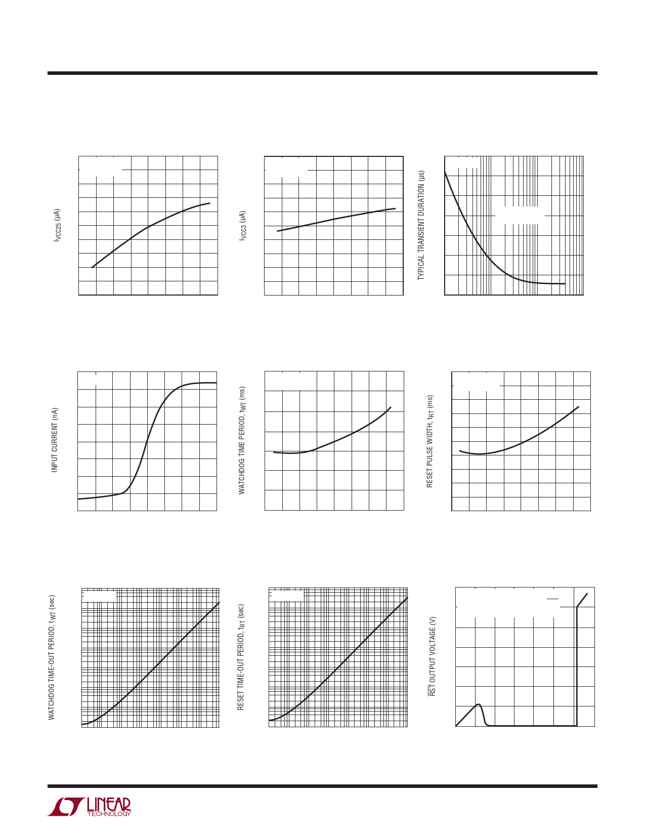
TYPICAL PERFOR A CE CHARACTERISTICS
LTC1726
Watchdog Time-Out Period vs
Capacitance
1000
100
TA = 25°C
10
1
100m
10m
1m
100µ
1p
10p 100p 1n 10n 100n
CWT (FARAD)
1µ 10µ
1726 G12
Reset Time-Out Period vs
Capacitance
100
TA = 25°C
10
1
100m
10m
1m
100µ
10µ
1p
10p 100p 1n 10n 100n
CRT (FARAD)
1µ 10µ
1726 G15
RST Output Voltage vs
Supply Voltage (LTC1726-2.5)
VCC3 = VCC25 = VCCA
3
10k PULL-UP FROM VCC3 TO RST
TA = 25°C
2
1
0
0
1
2
3
VCC3 (V)
1726 F13
PI FU CTIO S
VCC3 (Pin 1): 3.3V Sense Input. This pin also supplies
power to the part when the voltage on this pin is greater
than the voltage on VCC25/VCC5. Bypass this pin to ground
with a 0.1µF or larger ceramic capacitor.
VCC5 (Pin 2): 5V Sense Input (LTC1726-5). This pin also
supplies power to the part when the voltage on this pin is
greater than the voltage on VCC3. Bypass this pin to
ground with a 0.1µF or larger ceramic capacitor.
VCC25 (Pin 2): 2.5V Sense Input (LTC1726-2.5). This pin
also supplies power to the part when the voltage on this
pin is greater than the voltage on VCC3. Bypass this pin to
ground with a 0.1µF or larger ceramic capacitor.
VCCA (Pin 3): 1V Sense, High Impedance Input. If unused
it can be tied to either VCC3, VCC5 or VCC25.
GND (Pin 4): Ground.
WDI (Pin 5): Watchdog Input. A logic input whose rising
or falling edge must occur on this pin within the selected
watchdog time-out period or a reset pulse will occur. The
watchdog time-out period is set by the value of the
capacitor that is placed on the WT pin. The rising or falling
edge of this pin clears the voltage on the WT capacitor,
preventing a reset pulse from occurring. If the watchdog
timer is not cleared, a reset pulse will occur. The watch-
dog timer is cleared during a reset and restarts when the
reset is deasserted. When disabling the watchdog func-
tion, this pin should be connected to either VCC3 or
ground and WT must be grounded.
RST (Pin 6): Reset Logic Output. Active low, open-drain
logic output with weak pull-up to VCC3. Asserted when
one or more of the supplies are below trip thresholds.
After all supplies become valid, the reset remains as-
serted for the period set by the capacitor on the RT pin.
The watchdog timer can also trigger the reset whenever
the watchdog time-out period is exceeded. This pin can
be pulled up greater than VCC3 when interfacing to 5V
logic.
WT (Pin 7): Watchdog Time-Out Input. Place a capacitor
between this pin and ground to adjust the watchdog time-
out period. To determine the watchdog time-out period:
tWT = 21.8 • CWT
with tWT in µs and CWT in pF. As an example, a 47nF
capacitor will generate a 1s watchdog time-out period.
The watchdog function can be disabled by connecting
this pin to ground.
1726fb
5
Share Link: