LTC1741IFW データシートの表示(PDF) - Linear Technology
部品番号
コンポーネント説明
メーカー
LTC1741IFW Datasheet PDF : 20 Pages
| |||
LTC1741
ABSOLUTE MAXIMUM RATINGS
OVDD = VDD (Notes 1, 2)
Supply Voltage (VDD) ............................................. 5.5V
Analog Input Voltage (Note 3) .... – 0.3V to (VDD + 0.3V)
Digital Input Voltage (Except OE)
(Note 3) .................................. – 0.3V to (VDD + 0.3V)
OE Input Voltage (Note 4) ............ –0.3V to (VDD + 0.3V)
Digital Output Voltage ................. – 0.3V to (VDD + 0.3V)
OGND Voltage ..............................................– 0.3V to 1V
Power Dissipation ............................................ 2000mW
Operating Temperature Range
LTC1741C ............................................... 0°C to 70°C
LTC1741I ............................................ – 40°C to 85°C
Storage Temperature Range ................. – 65°C to 150°C
Lead Temperature (Soldering, 10 sec).................. 300°C
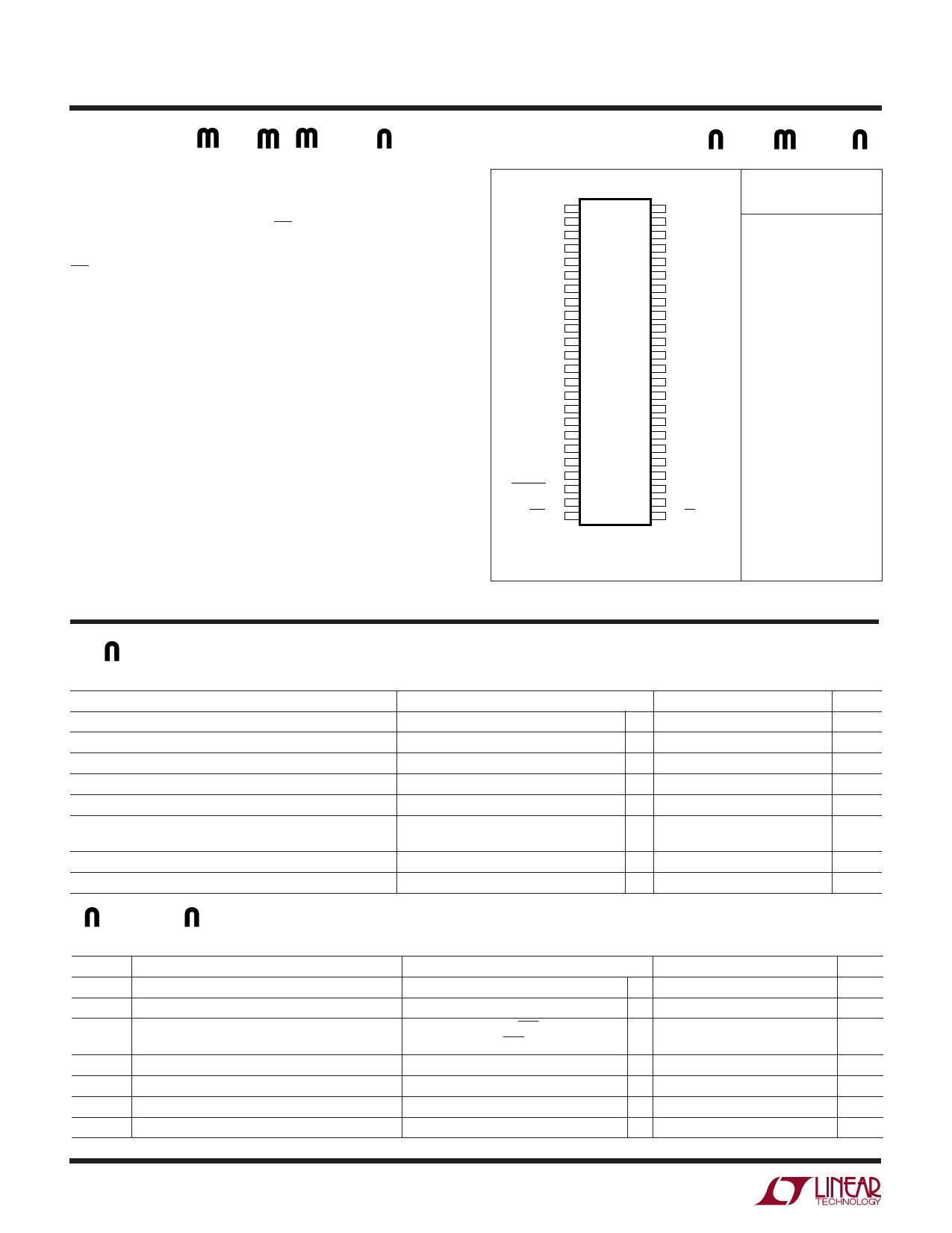
PACKAGE/ORDER INFORMATION
TOP VIEW
SENSE 1
VCM 2
GND 3
AIN+ 4
AIN– 5
GND 6
VDD 7
VDD 8
GND 9
REFLB 10
REFHA 11
GND 12
GND 13
REFLA 14
REFHB 15
GND 16
VDD 17
VDD 18
GND 19
VDD 20
GND 21
MSBINV 22
ENC 23
ENC 24
48 OF
47 OGND
46 D11
45 D10
44 D9
43 OVDD
42 D8
41 D7
40 D6
39 D5
38 OGND
37 GND
36 GND
35 D4
34 D3
33 D2
32 OVDD
31 D1
30 D0
29 NC
28 NC
27 OGND
26 CLKOUT
25 OE
FW PACKAGE
48-LEAD PLASTIC TSSOP
TJMAX = 150°C, θJA = 35°C/W
ORDER PART
NUMBER
LTC1741CFW
LTC1741IFW
Consult LTC Marketing for parts specified with wider operating temperature ranges.
CO VERTER CHARACTERISTICS The q indicates specifications which apply over the full operating
temperature range, otherwise specifications are at TA = 25°C. (Note 5)
PARAMETER
CONDITIONS
MIN TYP MAX
UNITS
Resolution (No Missing Codes)
q
12
Bits
Integral Linearity Error
(Note 6)
q
–1
±0.4
1
LSB
Differential Linearity Error
q –0.8 ±0.2
0.8
LSB
Offset Error
(Note 7)
– 35
±5
35
mV
Gain Error
External Reference (SENSE = 1.6V)
– 3.5
±1
3.5
%FS
Full-Scale Drift
Internal Reference
External Reference (Sense = 1.6V)
±40
ppm/°C
±20
ppm/°C
Offset Drift
±20
µV/°C
Input Referred Noise (Transition Noise)
Sense = 1.6V
0.21
LSBRMS
A ALOG I PUT The q indicates specifications which apply over the full operating temperature range, otherwise
specifications are at TA = 25°C. (Note 5)
SYMBOL PARAMETER
CONDITIONS
MIN
TYP
MAX UNITS
VIN
Analog Input Range (Note 8)
IIN
Analog Input Leakage Current
CIN
Analog Input Capacitance
4.75V ≤ VDD ≤ 5.25V
Sample Mode ENC < ENC
Hold Mode ENC > ENC
q
±1 to ±1.6
V
q –1
1
µA
8
pF
4
pF
tACQ
tAP
tJITTER
CMRR
Sample-and-Hold Acquisition Time
Sample-and-Hold Acquisition Delay Time
Sample-and-Hold Acquisition Delay Time Jitter
Analog Input Common Mode Rejection Ratio
1.5V < (AIN– = AIN+) < 3V
q
5
7.3
ns
0
ns
0.15
psRMS
80
dB
1741f
2
Share Link: 