LTC1751 データシートの表示(PDF) - Linear Technology
部品番号
コンポーネント説明
メーカー
LTC1751 Datasheet PDF : 12 Pages
| |||
LTC1751/LTC1751-3.3/LTC1751-5
ELECTRICAL CHARACTERISTICS The q denotes specifications which apply over the full specified
temperature range, otherwise specifications are at TA = 25°C. CFLY = 1µF, CIN = 10µF, COUT = 10µF unless otherwise noted.
SYMBOL PARAMETER
CONDITIONS
MIN TYP MAX
UNITS
LTC1751-3.3/LTC1751-5
UVL
PGOOD Undervoltage Low Threshold
UVH
PGOOD Undervoltage High Threshold
VOL
PGOOD Low Output Voltage
IOH
PGOOD High Output Leakage
LTC1751/LTC1751-3.3/LTC1751-5
Relative to Regulated VOUT (Note 6)
Relative to Regulated VOUT (Note 6)
IPGOOD = – 500µA
VPGOOD = 5.5V
q –11
–7
–3
%
q –8
– 4.5
–2
%
q
0.4
V
q
1
µA
ISHDN
Shutdown Supply Current
VIN ≤ 3.6V, VOUT = 0V, VSHDN = 0V
3.6V < VIN, VOUT = 0V, VSHDN = 0V
q
0.01
2
µA
q
5
µA
VIH
SHDN Input Threshold (High)
q 1.5
V
VIL
SHDN Input Threshold (Low)
q
0.3
V
IIH
SHDN Input Current (High)
SHDN = VIN
q –1
1
µA
IIL
SHDN Input Current (Low)
SHDN = 0V
q –1
1
µA
tr
VOUT Rise Time
VIN = 3V, IOUT = 0mA, 10% to 90% (Note 6)
0.6ms/nF • CSS
sec
fOSC
Switching Frequency
Oscillator Free Running
800
kHz
Note 1: Absolute Maximum Ratings are those values beyond which the life
of a device may be impaired.
Note 2: Based on long term current density limitations.
Note 3: The LTC1751EMS8-X is guaranteed to meet performance
specifications from 0°C to 70°C. Specifications over the – 40°C to 85°C
operating temperature range are assured by design, characterization and
correlation with statistical process controls.
Note 4: The no load input current will be approximately ICC plus twice the
standing current in the resistive output divider.
Note 5: ROUT ≡ (2VIN – VOUT)/IOUT.
Note 6: See Figure 2.
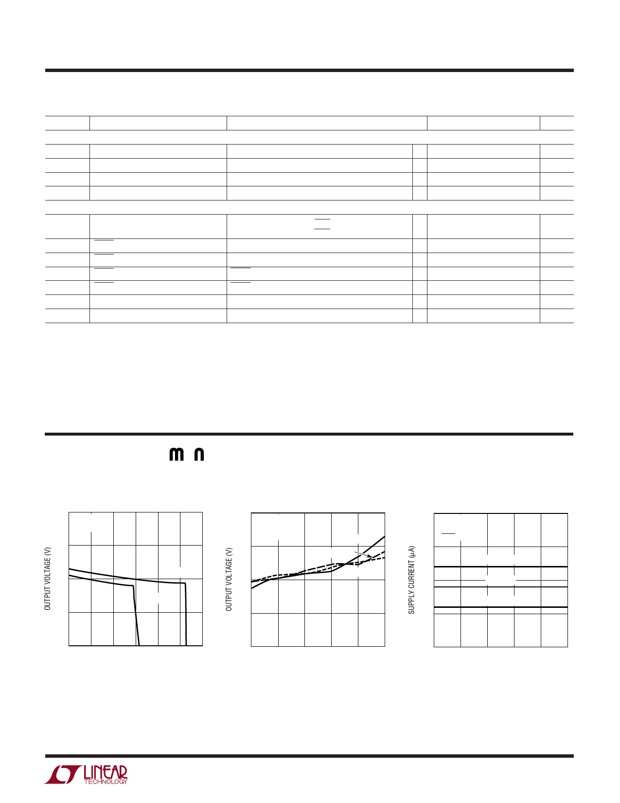
TYPICAL PERFOR A CE CHARACTERISTICS
(LTC1751-3.3)
Output Voltage vs Load Current
3.40
TA = 25°C
CFLY = 1µF
3.35
VIN = 2.5V
3.30
VIN = 2V
3.25
Output Voltage vs Input Voltage
3.40
IOUT = 40mA
CFLY = 1µF
COUT = 10µF
3.35
TA = –40°C
TA = 25°C
TA = 85°C
3.30
3.25
3.20
0
25 50 75 100 125 150
LOAD CURRENT (mA)
1751 G01
3.20
2.0
2.5 3.0 3.5 4.0 4.5
INPUT VOLTAGE (V)
1751 G02
No Load Supply Current
vs Input Voltage
40
IOUT = 0mA
CFLY = 1µF
VSHDN = VIN
30
TA = 85°C
20
TA = 25°C
TA = –40°C
10
0
2.0 2.5 3.0 3.5 4.0 4.5
INPUT VOLTAGE (V)
1751 G03
3
Share Link: 