LTC1773EMS データシートの表示(PDF) - Linear Technology
部品番号
コンポーネント説明
メーカー
LTC1773EMS Datasheet PDF : 20 Pages
| |||
LTC1773
ABSOLUTE AXI U RATI GS
(Note 1)
Input Supply Voltage .............................. –0.3V to 10.0V
ITH Voltage ................................................ –0.3V to 2.5V
RUN/SS, VFB, SENSE– Voltages .................. –0.3V to VIN
SYNC/FCB Voltage ...................................... –0.3V to VIN
BG, TG Voltages...........................................–0.3V to VIN
SW Voltage ...................................................– 5V to 11V
Operating Ambient Temperature Range
(Note 2) ...............................................–40°C to 85°C
Junction Temperature (Note 3) ............................. 125°C
Storage Temperature Range ..................–65°C to 150°C
Lead Temperature (Soldering, 10 sec.)................. 300°C
UW U
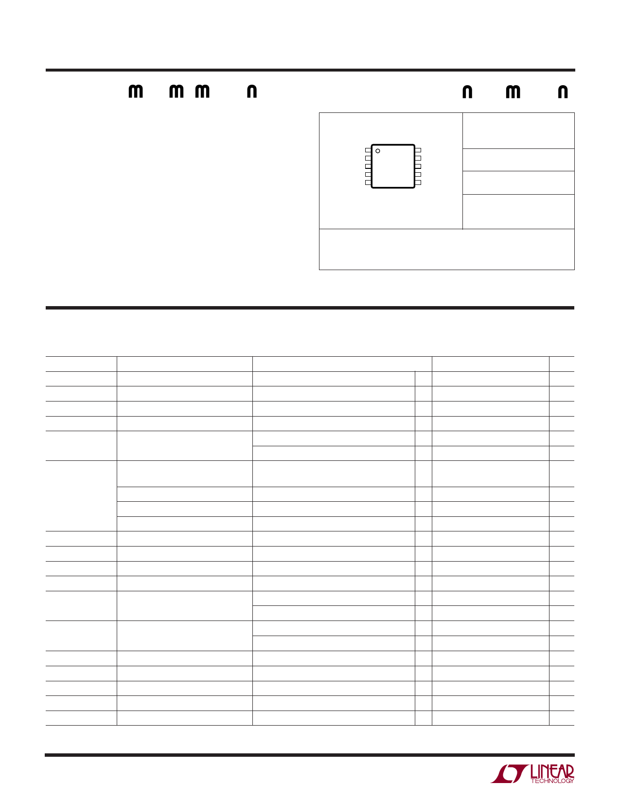
PACKAGE/ORDER I FOR ATIO
ITH 1
RUN/SS 2
SYNC/FCB 3
VFB 4
GND 5
TOP VIEW
10 SW
9 SENSE–
8 VIN
7 TG
6 BG
MS PACKAGE
10-LEAD PLASTIC MSOP
TJMAX = 125°C, θJA = 120°C/W
ORDER PART
NUMBER
LTC1773EMS
MS PART MARKING
LTMV
Order Options Tape and Reel: Add #TR
Lead Free: Add #PBF Lead Free Tape and Reel: Add #TRPBF
Lead Free Part Marking: http://www.linear.com/leadfree/
Consult LTC Marketing for parts specified with wider operating temperature ranges.
ELECTRICAL CHARACTERISTICS The ● denotes specifications which apply over the full operating
temperature range, TA = 25°C. VIN = 5V unless otherwise specified.
SYMBOL
IVFB
VFB
∆VOVL
∆VFB
VLOADREG
IS
VRUN/SS
IRUN/SS
VSYNC/FCB
ISYNC/FCB
fOSC
VUVLO
∆VSENSE(MAX)
TG tr
TG tf
BG tr
BG tf
PARAMETER
Feedback Current
Regulated Feedback Voltage
∆Output Overvoltage Lockout
Reference Voltage Line Regulation
Output Voltage Load Regulation
Input DC Bias Current
Normal Mode
Burst Mode Operation
Shutdown
Shutdown
RUN/SS Threshold
Soft-Start Current Source
Auxiliary Feedback Threshold
SYNC/FCB Pull-Up Current
Oscillator Frequency
Undervoltage Lockout
Top Gate Drive Rise Time
Top Gate Drive Fall Time
Bottom Gate Drive Rise Time
Bottom Gate Drive Fall Time
CONDITIONS
MIN TYP MAX
(Note 4)
20
60
(Note 4)
● 0.788 0.80 0.812
∆VOVL = VOVL – VFB
VIN = 2.7V to 8.5V (Note 4)
ITH at 1.0V (Note 4)
ITH at 0.6V (Note 4)
(Note 5)
VIN = 5V, VITH = OPEN, VSYNC/MODE = OPEN
VITH = 0V, VIN = 5V, VSYNC/MODE = OPEN
VRUN/SS = 0V, 2.7V < VIN < 8.5V
VRUN/SS = 0V, VIN < 2.4V
40
60
80
0.002 0.02
0.2
0.8
–0.2 –0.8
400 600
80
10
30
2
5
0.4
0.7
1.0
VRUN/SS = 0V
VSYNC/FCB Ramping Negative
VSYNC/FCB = 0V
VFB = 0.8V
VFB = 0V
VIN Ramping Down from 3V
VIN Ramping Up from 0V
Maximum Current Sense Voltage
0.75
1.5
2.5
0.76
0.8
0.84
0.1
0.4
1.0
500 550 600
55
● 2.35
2.5
2.65
●
2.65
2.8
● 85
100 115
CLOAD = 3000pF (Note 6)
CLOAD = 3000pF (Note 6)
CLOAD = 3000pF (Note 6)
CLOAD = 3000pF (Note 6)
45
160
48
150
80
180
45
150
UNITS
nA
V
mV
%/V
%
%
µA
µA
µA
µA
V
µA
V
µA
kHz
kHz
V
V
mV
ns
ns
ns
ns
1773fb
2
Share Link: 