LTC1773EMS データシートの表示(PDF) - Linear Technology
部品番号
コンポーネント説明
メーカー
LTC1773EMS Datasheet PDF : 20 Pages
| |||
LTC1773
PIN FUNCTIONS
ITH (Pin 1): Error Amplifier Compensation Point. The
current comparator threshold increases with this control
voltage. Nominal voltage range for this pin is 0V to 1.2V.
Under high duty cycle and nearing current limit, ITH can
swing up to 2.4V.
RUN/SS (Pin 2): Combination of Soft-Start and Run
Control Inputs. A capacitor to ground at this pin sets the
ramp time to full current output. The time is approximately
0.8s/µF. Forcing this pin below 0.4V shuts down all the
circuitry.
SYNC/FCB (Pin 3): Multifunction Pin. This pin performs
three functions: 1) secondary winding feedback input, 2)
external clock synchronization and 3) Burst Mode opera-
tion or forced continuous mode select. For secondary
winding applications, connect to a resistive divider from
the secondary output. To synchronize with an external
clock, apply a TTL/CMOS compatible clock with a fre-
quency between 585kHz and 750kHz. To select Burst
Mode operation, tie SYNC/FCB to VIN. Grounding this pin
forces continuous operation.
VFB (Pin 4): Feedback Pin. Receives the feedback voltage
from an external resistive divider across the output. Do not
use more than 0.01µF of feedforward capacitance from FB
to the output.
GND (Pin 5): Ground Pin.
BG (Pin 6): Bottom Gate Driver of External N-Channel
Power MOSFET. This pin swings from 0V to VIN.
TG (Pin 7): Top Gate Driver of External P-Channel Power
MOSFET. This pin swings from 0V to VIN.
VIN (Pin 8) : Main Supply Pin. Must be closely decoupled
to GND (pin 5).
SENSE–(Pin 9): The Negative Input to the Current Com-
parator. A sense resistor between this pin and VIN sets the
peak current in the top switch. Connect this pin to the
source of the external P-Channel power MOSFET.
SW (Pin 10): Switch Node Connection to Inductor. This
pin connects to the drains of the external main and
synchronous power MOSFET switches.
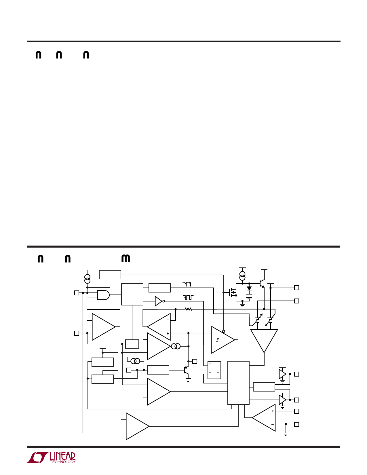
W
FUNCTIONAL DIAGRA
0.4µA
SYNC/FCB 3
BURST Y
DEFEAT
X
OSC
Y = “0” ONLY WHEN X IS A CONSTANT “1”
SLOPE
COMP
8 VIN
0.4V
9 SENSE–
VFB 4
0.6V –
SYNC
DEFEAT
+
0.8V REF
UVLO
TRIP = 2.5V
SHUTDOWN
0.8V
FREQ
SHIFT
+
EA
–
1.5µA
2
RUN/SS
RURNU/SNO/ FT
SOFSTT-ASRTATRT
0.86V
–
OVDET
+
0.22V
ITH
1
0.8V –
FCB
+
Figure 2.
EN
–
50mV
SLEEP
+
BURST
COMP
–+
ICOMP
SQ
RQ
SWITCHING
LOGIC
AND
BLANKING
CIRCUIT
ANTI
SHOOT-THRU
IRCMP
7 TG
6 BG
10 SW
5 GND
1773 FD
1773fb
5
Share Link: 